This thread has been locked.

If you have a related question, please click the "Ask a related question" button in the top right corner. The newly created question will be automatically linked to this question.

ADC08D1520 Differential Input Question

Other Parts Discussed in Thread: ADC08D1520, LMH6553

Hello,

A customer has the following question about what specifically does the ADC08D1520 input pins measure when it is provided with a differential input.

"I would like to be sure the input voltage is within the ADC signal input dynamic range. As such, I want to be certain what the ADC input is measuring."

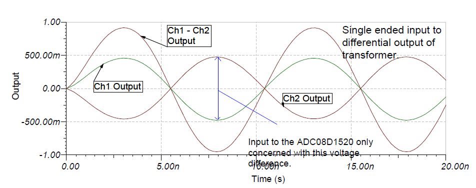
To illustrate this point, they made a SPICE simulation using a generic transformer to produce a different output from a single-ended input.

Their understanding is that the ADC is measuring the potential difference between the two signals, and want to be sure that such a measurement can be used in order to ensure that the differential voltage is within the ~560 mV or ~ 840 mV limit of the part.

They also have Ch1 - Ch2 on the SPICE simulation, but the understanding is that this measurement is not performed by the ADC. Is that correct?

Is the input of the ADC08D1520 only concerned with the voltage differential illustrated below?

SPICE Simulation Waveform:

SPICE Model:

  • Hi Ralph

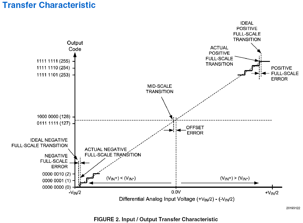
    This diagram may help to understand the differential input transfer characteristics and input range. Let's use the minimum extended control mode (ECM) value of 560mVp-p differential for example.

    Since this value is quoted in peak-to-peak differential units, that means that when the input is at -280mV differential (peak) the ADC output code is a 00000000. And when the input is at +280mV differential (peak), the ADC output code is at 11111111. Any differential voltage more than 1 lsb larger than +280mV or -280mV will cause the over-range (OR) output bit to be asserted.

    To use the customer Ch1 Output and Ch2 Output notation:

    In the first case (Ch1 Output - Ch2 Output) = -280mV.

    In the second case (Ch1 Output - Ch2 Output) = +280mV

    I hope this is helpful.

    Best regards,

    Jim B

  • Please correct me here. In the case above, if the input differential is greater than +280 mV (say +320 mV) , OR+ goes high and OR- goes low, indicating out of range. Does this mean the ADC output code reads 1111 1111? Same with -280 mV (say -320 mV), OR+ goes high and OR- goes low, indicating out of range, thus ADC output code reads 0000 0000.
  • Hi Peter

    You are correct in both cases.

    Best regards,

    Jim B

  • Lets say you are using a perfect single ended-to-differential transformer. So one should always get half the signal above 0V (the + half), and half the signal below 0V (the - half), thus evenly spread across the scale above. The differential voltage potential across Vin+ and Vin- is simply double either half (looking at magnitudes only). If you subtract (Vin+) from -(Vin-), it seems you will always get 0.0V on the horizontal axis above, so I am missing something here.
  • Hi Peter

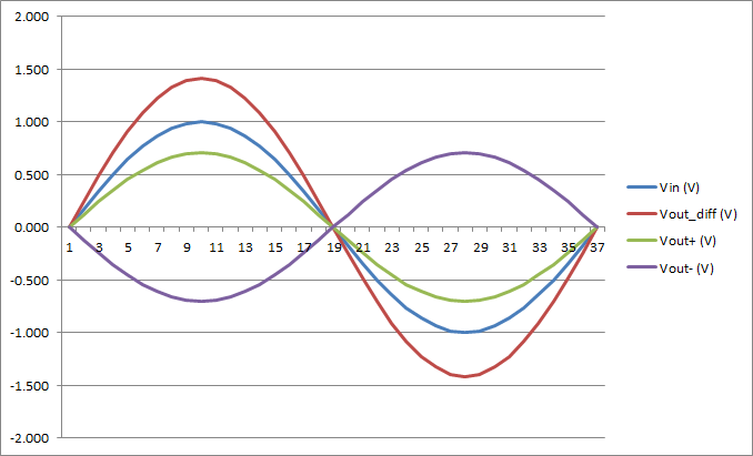
    The plot below shows the case you are describing. Vin is the 50 ohm Single Ended input. Vout_diff is the 100 ohm differential output (Vout+ - Vout-). For an ideal balun, the instantaneous power in and power out are equal, so the output voltage can be calculated using the input power (Vin^2 / 50ohms) and the 100 ohm output impedance.

    The outputs of the balun are centered around 0V. Since the ADC differential inputs must be at the proper common mode voltage (Vcmi) the balun output must be AC coupled to the self-biased ADC inputs. The differential swing will be the same, but the absolute voltages will be shifted up by Vcmi.

    The ADC input responds to the Vout_diff voltage (reddish color above). When this is positive the ADC codes are above mid-scale (1000 0000 to 1111 1111 for the ADC08D1520). When, this signal is negative the ADC codes are below mid-scale (0000 0000 to 1000 0000 for the ADC08D1520).

    The spreadsheet attached here shows the information used to make this plot.

    1524.1to2 Impedance Ratio Transformer Voltages 2.xlsx

    I hope this helps.

    Best regards,

    Jim B


  • Jim,
    Just to reiterate:
    1. The ADC input responds to Vout_diff.
    2. Vout_diff is shifted up by Cmi (approximately 1.26V since Cmi ~ Cmo).
    3. Cmi now establishes mid-scale. Positive ADC codes are above mid-scale, negative codes are below mid-scale.
    4. If Vout_diff is greater than approximately 650/2 mV (or 870/2 mV depending on FSR setting), or less than -650/2 (or -870/2 mV), output is clipped and ADC codes will be 1111 1111 or 0000 0000.

    Thank You.
  • Jim,

    For single ended applications where a balun or amplifier has to be used, what is the preferred method of voltage limiting into the ADC?

    1. For a balun, two diode limiters downstream of the transformer, but before the DC blocking capacitors, each straddling Vin+ and Vin- but with Anode/Cathode in opposite directions.

    or

    2. Use the LM6555 as in Figure 13 of the ADC08D1520 specification sheet.

    Thanks.
  • Hi Peter

    Option 1 is a good straightforward approach. A variety of limiting diode type products are available for that configuration.

    If Option 2 is used, care must still be taken to ensure the output of the amplifier does not exceed the input voltage and current limits of the ADC. Another approach is to use a product like the LMH6553, which has an adjustable output limiting clamp feature.

    Best regards,

    Jim B

  • Jim,
    We plan to use option 1 circuit as outlined in the previous threads. As stated above, the ADC responds to Vout_diff, so if the input is greater than FSR/2 the ADC will clip. For example, if FSR is set to 650 mV, and my input sine wave test signal is greater than 325 mV peak-to-peak, the ADC will clip (don't forget I am going single ended to differential using a transformer). Does TI have any recommendations as to the limiter types (vendor/model #) that will allow me to limit the input differential signal to around 325 mV? Thanks.
  • Hi Peter

    I don't know of any off-hand that limit at that precise (and low) voltage level.

    Please keep in mind that it is OK to have the input signal go beyond the FS+ and FS- levels, but to maintain device reliability the limits listed in the Operating Ratings section of the datasheet must be followed.  These are the limits you should be planning around with your limiter selection.

    Best regards,

    Jim B