This thread has been locked.

If you have a related question, please click the "Ask a related question" button in the top right corner. The newly created question will be automatically linked to this question.

The 500MHz noise of ADC08d1020

Other Parts Discussed in Thread: LMX2541, ADC08D1020, ADC08D1520

Hi,all

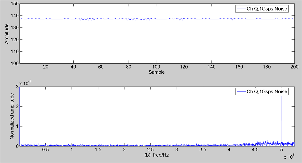
Now i am using ADC08D1020 for data acquisition at 1Gsps.I find that there is a  500MHz noise in signal.I think this may comes from the interference of ADC clock which is supported by LMX2541. The  frequency domain digram of the noise is as follows. I hope you can give me some advice.

Best Regards.

  • Hi zh

    In the ADC08D1020, each internal I and Q converter is made up of two interleaved sub-convertters (I1,I2 and Q1,Q2). Additionaly, a calibrated ADC design is used. The calibration process optimizes offset, gain and linearity of the internal sub-converters. Therefore it is important that the device calibration is done to ensure the device performance meets the datasheet specifications.

    After the ADC is powered on, allow the temperature to stabilize and then calibrate the ADC by toggling the CAL input pin low then high, or by setting the CAL bit low then high, as directed in the datasheet, making sure to observe the minimum required low and high times. Calibrating the ADC will optimize the internal offsets and linearity of the sub-converters. Once calibrated, there may still be some small residual offset mismatch between the interleaved subconverters, but the mismatch will be small enough that the device does meet datasheet specifications.

    Please ensure the ADC is being calibrated under the final operating conditions. If the observed noise at Fs/2 is still higher than expectations please send a raw data file (single column data text file in decimal or hex format).

    Best regards,

    Jim B

  • Hi,Jim

    Thanks for your relay.

    1. I checked  my design to make sure the calibration of the device. The calibration procedures are described below.

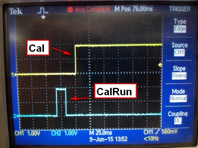
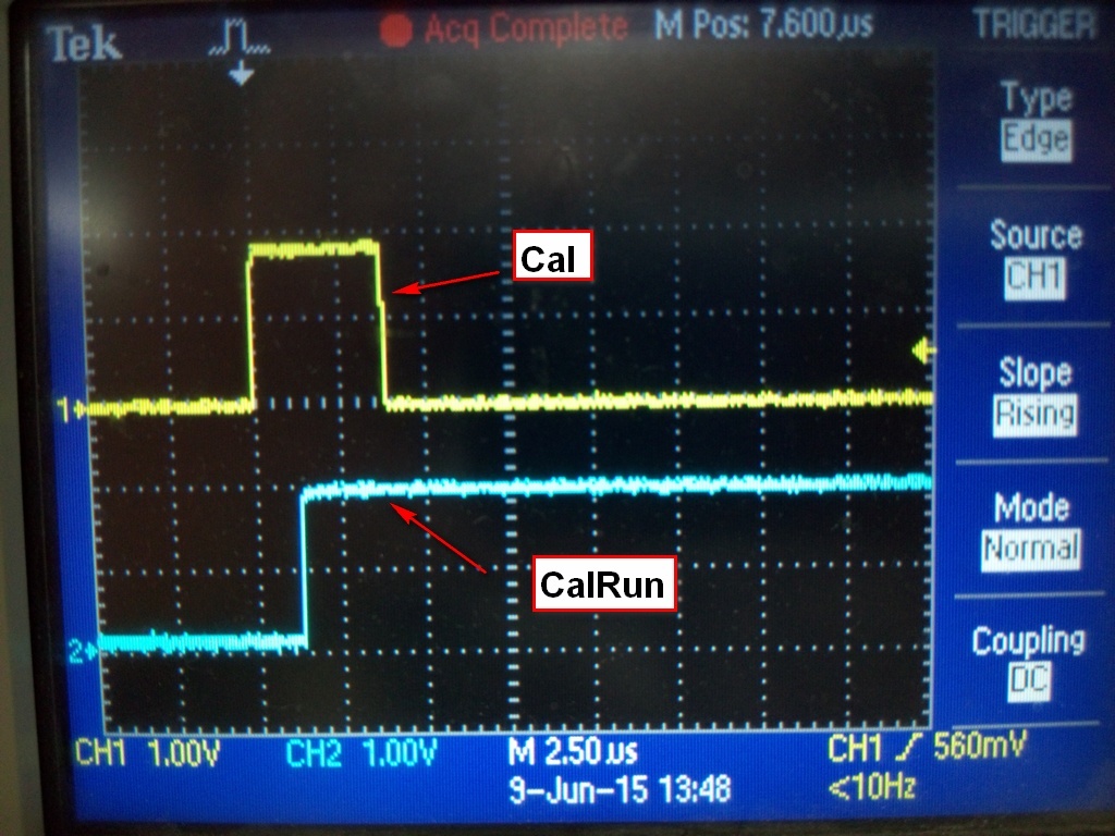
    1>. Because ADC power up first than FPGA,when ADC power on ,the cal pin is low and power-on calibraion will be performed. when become to configurate FPGA, the Cal pin becomes high.(Cal and Calrun  pin are connected to FPGA)

    2>. When  the configuration of FPGA finished, the FPGA  pull the cal pin low for 20s,then pull the cal pin high to trig ADC on-command calibration.

    2.According  my test ,now  the I channel noise is worse than the Q channel . The raw data files are attached below.

    Ich.txt

    Qch.txt

    Looking forward your reply.

    Thank you very much.


  • Hi zh

    Your calibration process looks correct. The only added recommendation is to make sure the ADC has fully warmed up to operating temperature before doing the final calibration and beginning to use the device. I normally recommend re-calibrating after the device has been powered up with stable clock signal applied for at least 1 minute.

    I see the higher amount of toggling on the I-channel data you provided, which does appear to related to even/odd samples. The even/odd sample differences may be due to the fact that the I and Q converters are each implemented using 2 internal sub-converters. In effect there are internal converters I1, I2 and Q1, Q2. These internal sub-converters take turns sampling the input signal, each operating at half the sample rate of the full converter channel. For example at 1 GSPS, each internal sub-converter is operating at 500 MSPS, one sampling even samples, and the other the odd samples.

    After the ADC is calibrated, there can be small offset mismatches between the internal subconverters. This offset mismatch can lead to the data toggling you see. Even if the mismatch is less than 1-lsb, the toggling effect may be seen depending on the level of an applied DC signal, or the Offset Adjustment register value for that channel.

    I would suggest making sure the calibration has been done after sufficient warm-up time with clock active. Other factors that can affect the interleave converter offsets are the clock amplitude and connection. The clock inputs must be AC-coupled differential signals. The amplitude of the clock must be within the recommended amplitude range specified in the datasheet. If the clock is too large that can sometimes cause increased offsets or noise in the interleaved sub-converter data.

    Unfortunately I am traveling and don't have an ADC08D1X20 board available to take comparative measurements right now. I should be able to take some measurements on Thursday if needed.

    Best regards,

    Jim B


  • Hi,Jim

    So sorry to diturb your trip.

    I changed the on-command calibraion time and made sure the device warm-up time. The phenomenon has not been improved.

    Now I'm not convenient to test the clock signal now, but the clock schematic is the same as the evaluation board of ADC08D1520. I will test clock later.

    Every time the board power on, the phenomenon is different. Sometimes the noise is large and sometimes is small.

    I hope you can give more advice.

    Thank you very much.


  • Hi,Jim

    Recently, i did some test below.

    1> I use the test pattern of the ADC to test the link between the FPGA and ADC, and the data i get is the same as the datasheet.

    2> when LMX2541 output 200Mhz clock, the amplitude is about 800mvpp  tested at the ADC end.

    3> when I power down the Q channel by PDQ pin,the data I get from DQ is BD(hex) and DQd is FE(hex). I don't know if this is right.

    I hope you can give me some help.

    Best Regards.

    zh

  • Hi zh

    In both full chip power-down (PD pin is high) or Q-channel power-down (PDQ is high, PD is low) the affected outputs are placed in a high impedance state. Therefore the affected data outputs Dxx will not have any valid information.

    In your case, with PDQ high, the DQ and DQd outputs are in the high impedance state and the resulting data captured in the FPGA is meaningless.

    Best regards,

    Jim B