This thread has been locked.

If you have a related question, please click the "Ask a related question" button in the top right corner. The newly created question will be automatically linked to this question.

ADS5463EVM Glitching

Other Parts Discussed in Thread: ADS5463EVM, ADS5463

Hello,

I have been developing some RTL code to capture readings taken from an ADS5463 on ADS5463EVM, I have tracked down a problem when the ADC crosses the "zero" line (2048).  I have worked through my RTL for a number of days and have not found in logic problems.  I have also checked the hardware and it seems fine the board has not been electrically or thermally stressed in any way.  I'm left with the assumption that there is an issue with the ADC.

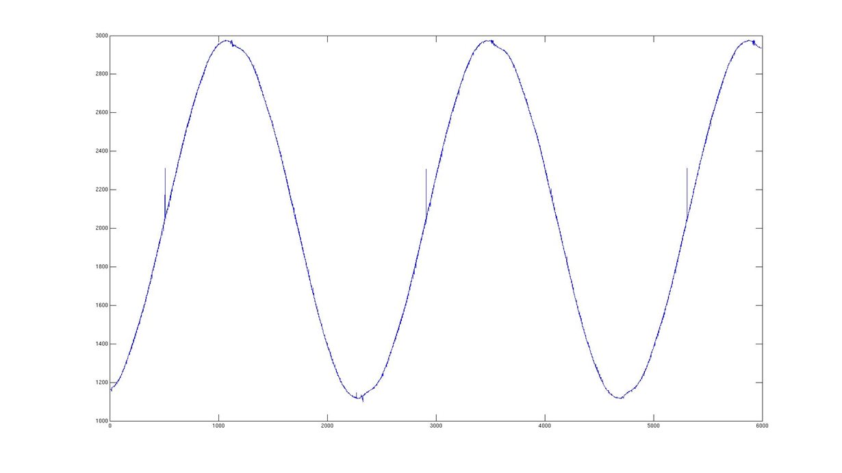
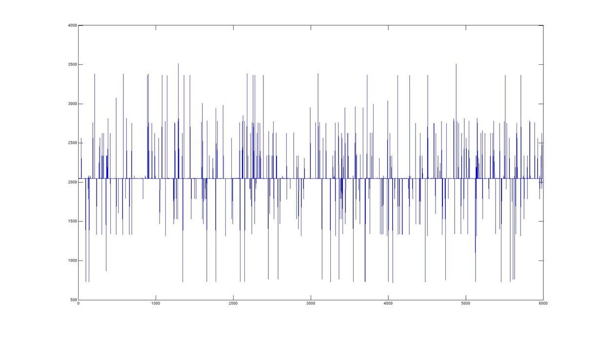
I have attached two graphs showing this error, first graph is from a not so clean sine wave at 166MHz and it is very easy to see the three spikes on the rising edge of the sine wave and the glitch occurs at the 2048 point.  The second graph is taken when the input have been tired to ground so I expect it to read a solid 2048 across the board but that is not what is happening.  The other case which I don't have a graph of right now is feeding in a steady voltage above zero produces a nice solid line at the appropriate level.

Steps I have taken to try and resolve the problem, I have tried various delay time from the DRY signal to when I latch the data but it does not seem to fix the zero crossing.

Any help that could be offered to point out an error in my thinking or the ADC would be greatly appreciated.

  • Hi,

    Let me address the second plot first, please.  If you have connected the two pins of the differential input to ground, then this is not within datasheet limits.  0V differential across the IN+ and IN- will result in an output code 2048 plus some random noise on the least significant bits plus some offset error, but only if the two pins are at the VCM voltage.  Even when looking for idle channel noise, the VCM specification must be followed.  If you connect the two input pins to each other and let them float to the VCM voltage or bias them up to the VCM voltage, you should then see a fairly flat capture of codes to within a few lsbs of random variation.

    So, what is the common mode level of the input signal?  Is the input AC coupled such that the ADC can bias the inputs up to its desired level, or if DC coupled is the signal biased up to where the ADC needs to see it?     And what is your sample rate, by the way?  Let's check VCM first and then come back to the glitches you see.

    Regards,

    Richard P.

  • Hi Richard,

    Thanks for the quick reply. Let me answer your questions to see if it helps determine the errors I'm seeing.

    My setup is a ADS5463EVM Evaluation Board with the default setup as it comes from the factory.  The input is transformer coupled, the VCM is 2.4V, and I'm using the non amplified input as well.  My sample rate is 400MSPS, and I'm capturing the data via a Cyclone V SoC, on an SoCKit development board.

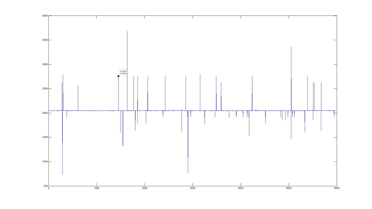
    I ran another test where instead of hooking the input signal to ground, I tested it with a shorted SMA connector and the below graph is the result.  It looks a little better than the graph above, but there is still some significant bit errors on the read out.

  • Hello Richard,

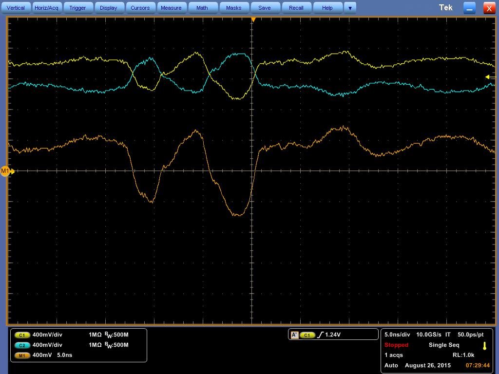
    I took some more readings on the ADS5463EVM board with the default factory configuration, through the transformer coupled input tied to the board ground via a shorted SMA connector.  This time I used the probe adapter that comes with the board and measured the individual bits coming directly from the ADC with an oscilloscope, that way it would total remove any doubt in my mind about my RTL capture code.  I'm still seeing the glitching or errors in the readings.  I have posted a screen grab from the oscilloscope with the above mentioned setup on bit D9(Yellow trace) and /D9(Blue trace), and it is clearly outputting a reading we it should not be.

  • Hi,

    Looking at your scope screenshot, why are you saying this clearly shows a glitch?  Is it because looking at bit 9 you would not expect any activity at all if the input channel is floating to VCM after the AC coupling for a 0V differential input?  (that is, idle channel noise)    With idle channel noise, we may or may not see all the bits toggle depending on the offset error the device has and the min to max spread of the sample codes in the idle channel noise.   For example, if the offset error for a device is 10 codes above 2048, but the span of idle channel noise id 7 codes above or below that - then there would be no transitions in the most significant bits.   The codes never cross the midscale.  But if the offset error was only 4 codes for example, then you would see all bits toggle when the code went from 1000 0000 0000 to 0111 1111 1111. 

    But in the example i just described, *all* the most significant bits toggle together.  When bit 9 goes from 0 to 1, so is bit 8 and bit 7 and so on.  I don't see that in your data captures.  It still could be an error in FPGA programming though, 'falling' edge bits aren't kept grouped and rising edge bits kept grouped, and the order is not preserved in which the rising edge bits and falling edge bits arrived at the input.  I've seen it happen.  One example was where two small FIFOs were used for the data from the IDDR cells, and occasional FIFO latency mismatches would mess up the order of the samples.   *That* error produces a characteristic signiture in the FFT of the data, and produces a classic 'sawtooth' pattern to the plot of the samples.   I do see a 'sawtooth' pattern in your first plot posted, where if you zoom in it looks like your sine wave has a down-up-down-up pattern all through the cycle, but only if some of the lsb's were swapped but not all 12 bits. 

    When you varied the delay between the data and your clock (DRY) what was your range of delay used?  The DRY signal is aligned with data transitions, so the DRY has to be delayed 90 degrees, or in your case 1.25ns in order to meet setup and hold time inside the FPGA.  When I was doing this with a Virtex4 some years ago, I found that the clock buffer used in the FPGA to route the clock to the IDDR cells added almost enough delay in and of themselves, leaving me to only need one r two more tap settings of delay on the clock using an IDELAY cell.   Cyclone V would have different timings than the Virtex4, but still - what is the magnitude of the delay you were using to sweep timing?  Maybe it was not enough.  I've also seen missing 100 ohm terminations in the FPGA cause strange results.

    If you could provide the serial number of the EVM in your possession then i could pull the plots that were saved during testing of your board,  The serial number may be inked in by hand in a blank white space provided for it, or on more recent builds it may be the last digits of a white sticker on the board.   Being a single channel ADC, the saved test data would be a single FFT plot, but a single FFT plot that meets data sheet SNR/SFDR specs would have to have the digital interface to the FPGA good.

    And of course, it is possible that something has been damaged, but that is not common.

    Regards,

    Richard P.

  • Hello Richard,

    You were right and you solved my issue. I mistakenly thought that assigning a pin as LVDS brought up the series resistor, but it does not. In addition to setting the pin as LVDS you also have to set it as differential to bring up the series resistor.

    "I've also seen missing 100 ohm terminations in the FPGA cause strange results." <-- Brilliant words.

    Thanks again for all the help!!
    Adam Perkins