This thread has been locked.

If you have a related question, please click the "Ask a related question" button in the top right corner. The newly created question will be automatically linked to this question.

ADC12D1600QML - RCLK

Hello TI,

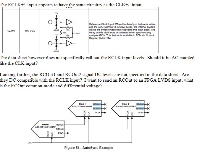
The RCLK+/- input appears to have the same circuitry as the CLK+/- input.  

The data sheet however does not specifically call out the RCLK input levels.  Should it be AC coupled like the CLK input? 


Looking further, the RCOut1 and RCOut2 signal DC levels are not specified in the data sheet.  Are they DC compatible with the RCLK input?  I want to send an RCOut to an FPGA LVDS input, what is the RCOut common-mode and differential voltage?  Refer to figure 51.  


Thanks,

Dan


  • Provided as an additional questions, not as an answer. I'm curious as well
  • Hi Dan and Wilson

    Regarding your RCLK and RCOut questions.

    1) The RCLK has similar input requirements to CLK, but is implemented slightly differently.

    2) RCOutx can be connected to RCLK inputs in either DC coupled or AC coupled fashion. AC coupled would be recommended if the ADCs were on different boards with possible DC voltage differences between the board grounds. AC coupling will work well as the RCLK in put has a built-in bias connection.

    3) The last point involved connecting RCOut to an FPGA LVDS input. The differential swing will be fine (typical is around 360mVpeak or 720mVpp). I'm still trying to track down what the typical output common mode voltage will be. I know I won't be able to provide a min/max for the common mode. The guaranteed way to make it work would be to AC couple from RCOut to the LVDS input and have 50kOhm resistors from the LVDS +/- inputs to a bias voltage that is centered in the input common mode range of the FPGA receiver.

    I hope this is helpful.

    Best regards,

    Jim B

  • Hi - I'm posting for Dan since he was having some trouble getting the image to show up properly.

    -----

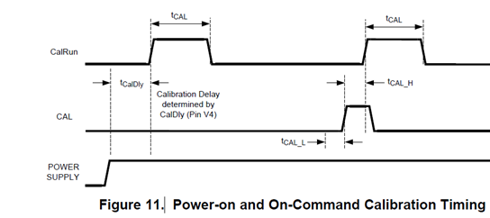
    In the ADC12D1600QML Figure 11 a "CalDly" term is used, but is mentioned no where else in the data sheet.  Pin V4 does not appear to have anything to do with calibration.

    My real question is whether there is any power supply rise time requirement other than that analog supply comes up as fast or faster than the others.

  • Figure 11 is an error in the datasheet. It is correct that this part does not have cal delay or power on reset. This will be corrected in the revision of the datasheet.
    There are no specific power up requirements.