This thread has been locked.

If you have a related question, please click the "Ask a related question" button in the top right corner. The newly created question will be automatically linked to this question.

ADS6149 explanation

Other Parts Discussed in Thread: ADS6149

Hello,

I would like to understand how ADS6149 runs.

I program the registers as below:

register 0x00h = 0x00h

register 0x20h = 0x00h

register 0x3Fh = 0x60h

register 0x41h = 0x40h

register 0x44h = 0x00h

register 0x50h = 0x03h

register 0x53h = 0x00h

register 0x55h = 0x00h

register 0x62h = 0x00h

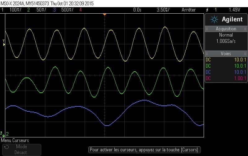
Then, you can fin in the below scope capture the signals.

Yellow signal, pin 10, CLKP

Green signal, pin 15, INNP

Blue Signal, pin 33, D0_D1_M

I don't understand the result on the pin 33. Could you give me advice or explanation?

Thanks

Best Regards

Nicolas Delabie

  • Nicolas,


    I've moved your post to the High Speed Data Converter Forum. The ADS6149 is supported through this forum, and I think you'll get an answer here.


    Joseph Wu
  • Hi,

    I cannot tell you much from the information provided,  From the scope screenshot, it looks like the sampling frequency is about 200MHz, but the waveform is not very steady from cycle to cycle.  Were you using a differential probe of adequate bandwidth across the differential pair of pins?  That would provide a much better idea of what the clock input looks like.

    At any rate, it also looks like the input signal at INNP is of equal frequency to the sampling clock.  If so, that would alias the input tone down to 0 Hz and the output sample bits should represent a constant sample value plus some noise on the least significant bits.

    But looking at the register list you provided: the data values for addresses 0x41 and 0x50 are invalid values for those registers.   And address 0x3F seems to set the device for external reference but you haven't stated what your external reference voltage is.

    That is about all I can say from what I see in the posting.

    Regards,

    Richard P.

  • Hi,
    In fact, there are erros on some registers. I modified the register 0x41 (new value 0x80h) and register 0x50 (new value 0x06h). Is it correct?
    Then, VCM (pin 13) is equal to 634mV. So is it correct for register 0x3F?
    I use passive probe. I measure between the signal and the GND.
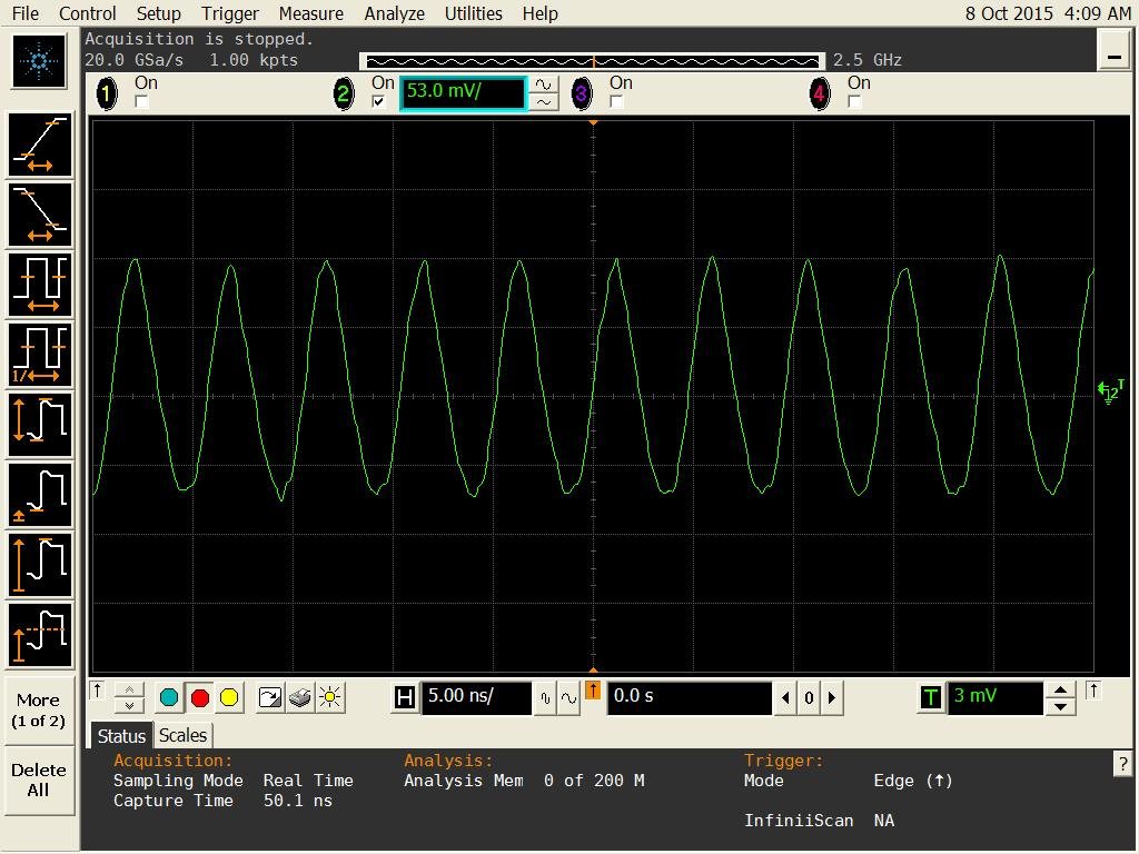
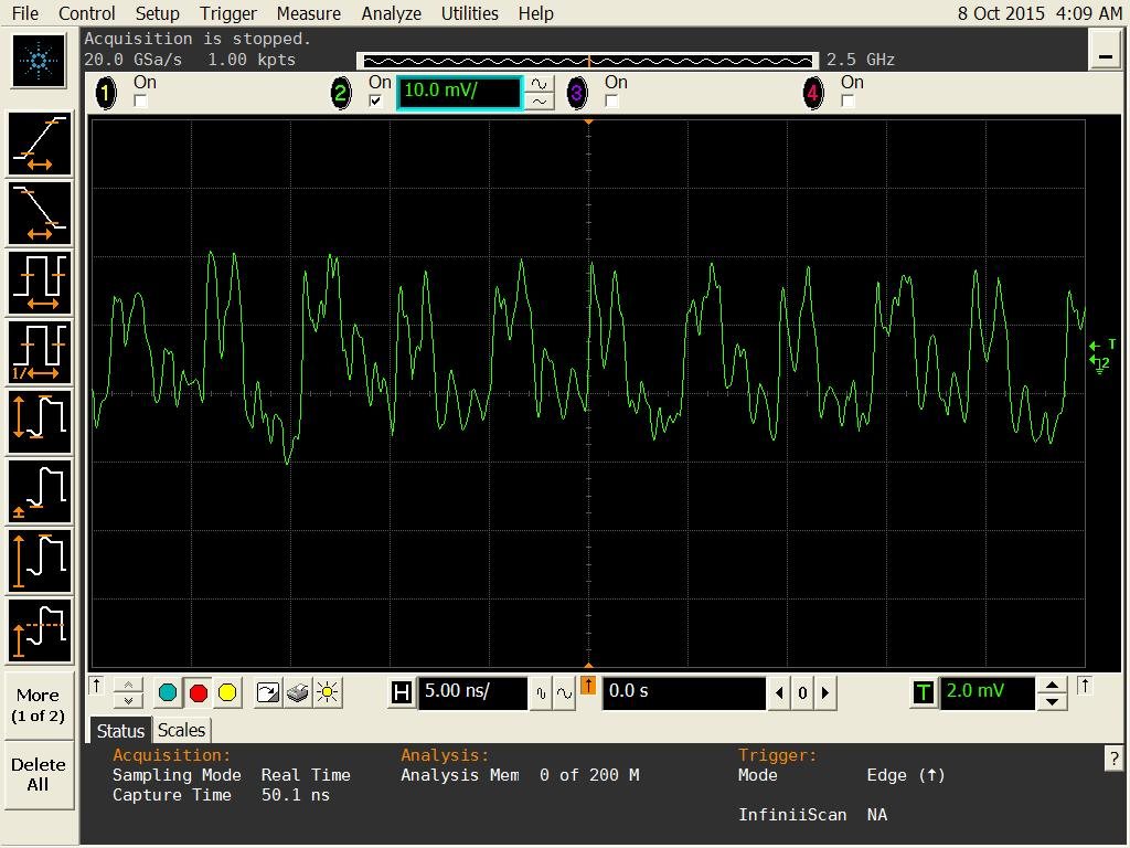
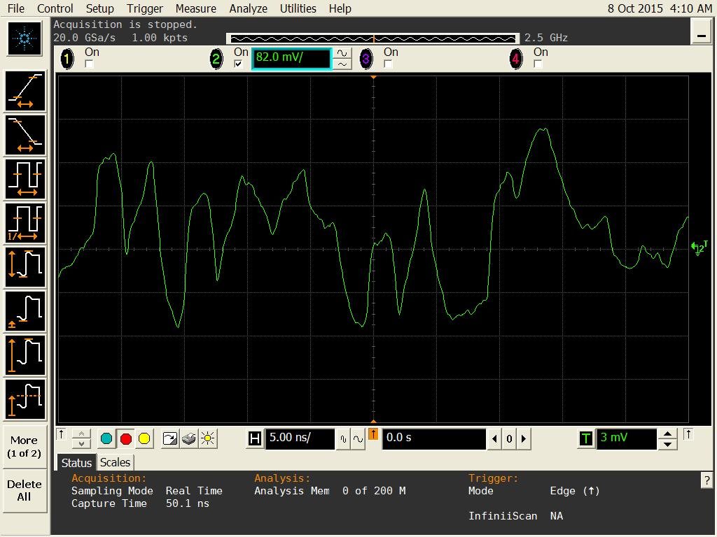
    The signal CLKP is equal to 208Mhz. About INP, the frequency should be 255Mhz. But there is some noise. You can find new measures of signals. I separately measured because I saw that there is some interference between CLKP and INP.
    I would like to know if the ADC is well configured?

    Regards

    Nicolas

    CLKP signal : 208 Mhz

    INP signal:

    Data 0 signal: