A related question is a question created from another question. When the related question is created, it will be automatically linked to the original question.
If you have a related question, please click the "Ask a related question" button in the top right corner. The newly created question will be automatically linked to this question.
You can program the registers in any order. The key to the DAC37J82 register is the alarm checking (i.e. such as PLL lock status) and the initialization sequence (i.e. 0x4A JESD204B intialization registers).
You may see the document link below for detail. This will be going to the latest DAC37J82 datasheet update
hello Kang,
Thanks for your quick response.
I have another question: how to calculate the DAC clk、 JESDclk and SERDES clk of DAC37j82? what is the computational formula of these clock?
my configuration : DAC37J82_2x_250MData_2lane_222mode_Fdac1000MHz_onchipPLLenable_inputclock250MHz.
look forward your reply.
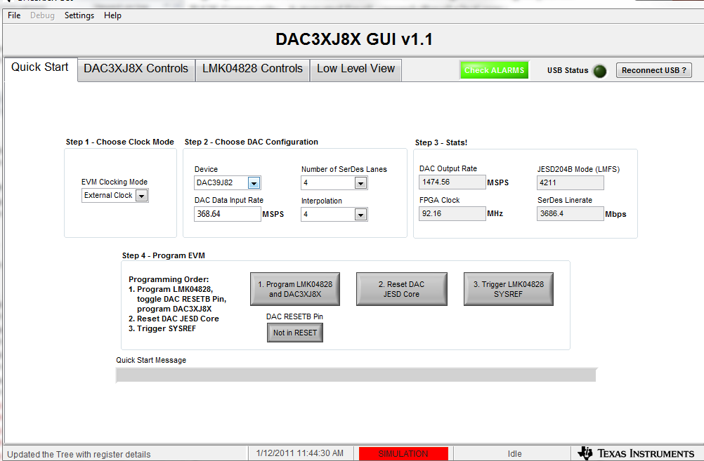
You may download the DAC3xJ8x EVM GUI. The main page provides all the calculation for the clocks, and the low level page tells you the equivalent register settings
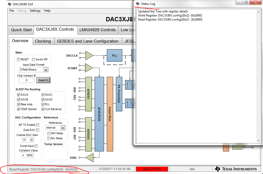
Yes, the GUI has a simulation mode that can work without an actual EVM board connected to the PC. In the simulation mode, you may view each register changes in the status log. Simply double click on the lower left hand corner and the status log will show up.
You may always load the register config file. The saving config feature works intermittently in this version. After you save, you may want to reload again to make sure it saves correctly.
To mask the alarms (i.e. alarms on register config100 to config109 do not show up on ALARM CMOS pin), you should set the alarms masking to "1b'1" in config4, config5, and config6.
To unmask the alarms (i.e. alarms on register config100 to config109 show up on ALARM CMOS pin), you should set the alarms masking to "1b'0" in config4, config5, and config6.
Now I can control the alarm pin. The next step is do JESD pattern test.
FPGA JESD core can send test pattern like /D.21.5/, /K.28.5/ etc.
While I'm doing that test, what registers should be checked to make sure if it's working?
I've checked config100~config109 and they are all 0 except config108 (it's read back as 0x7).
I uses 4 lane only and don't use DAC pll. So I thought it's working fine. But after changing test pattern to which different from FPGA, The register values of config100 ~ config109 are the same. ??
You may refer to the end of the following post for instructions of the JESD204B pattern test with Altera FPGA. This is a transport layer test so you have to make sure the physical layer (SERDES level) have to work fine.
According to DAC datasheet, I can select and check internal data.
But I couldn't find any details for jesd_testbus_selin the datasheet.
Could you help me out how to set up and which pin I need to check?
The following is from datasheet page 52(dac37j82.pdf).
Users can select to output the internal data (ex, the 8b/10 decoder output, comma alignment output, lane alignment output, frame alignment output, descrambler output, etc ) of a JESD link for test purpose. See jesd_testbus_sel for configuration details
I'm trying to test JESD data link layer with test pattern for example K.28.5.
According to datasheet, DAC will verify test pattern and report to alarm.
But I have no idea which register I should check.
The following is taken from datasheet.
Could you let me know which register has pass/fail test result?
jesd_test_seq Set to select and verify link layer test sequences. The error for these 00 sequences comes out the lane alarms bit0. 1= fail and 0 = pass. 00 : test sequence disabled 01 : verify repeating D.21.5 high frequency pattern for random jitter 10 : verify repeating K.28.5 mixed frequency pattern for deterministic jitter 11 : verify repeating ILA sequence
Enable the link layer test pattern through register jesd_test_seq in config74 (0x4A). Once the associated pattern is transmitted from the JESD204B TX logic device for the link layer pattern test, the error will be reflected on bit 8 of config100 to config107 for the respective JESD204B RX lane.
I have send this information to our tech write for the datasheet update.
The JESD_testbus_sel is meant to be a TI internal test only. The output of the internal data may not provide much meaningful result in terms of debugging your system. We are removing this from the datasheet moving forward.
You may ignore the Lane0~3 FIFO error during JESD pattern tests. You should only consider the FIFO error during normal operation of the DAC37J82. There is a FIFO stage between the JESD204B RX block and the digital logics of the DAC37J82. If the data rate between the two stages are mis-configured, the FIFO error will trigger.
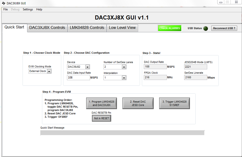
With higher multiplication ratio and lower reference clock frequency, the SERDES PLL are more sensitive to input reference clock jitter. I suspect by moving the reference clock from 108 to 216MHz the jitter performance becomes acceptable. We provide our DACCLK from high quality clock source such as the LMK04828. Please double check your clock source performance and maybe we can narrow it down.
We can also duplicate the setup here to see how 108MHz reference works for 2160Mbps of SERDES rate. I believe you are using the follow mode, please let me know if I misunderstood your setup:
I am not too familiar with the LMK03033, you can check with the clocking team on the clocking forum for their advise on this.
We can only check the setup with the on-board LMK04828 on our DAC EVM.
There is an error on the datasheet description and we are working on the datasheet update (it is scheduled to be completed by mid 2nd quarter)
for config108, 15:12 alarm_sysref_ err, each bit should be refer to link SYSREF error as oppose to lane error.
bit15 = link3
bit14 = link2
bit13 = link1
bit12 = link0
The DAC37J84 supports up to two independent JESD204B links (link0 and link1) Each link can have up to 4 lanes as long as the number of lanes in each link matches. The lane to link mapping is done in config73.
If the read back of error for these 4 bits are 0xC, then link1 and link0 do not have SYSREF error. By default, only link 0 is used. Link 1 is used in combination of link0 if some redundancy is needed in the system
I have confirmed on our TSW14J56 + DAC37j82 EVM that with quarter rate SERDES, the reference clock of 108MHz, multiplier of 20x would work. I also confirmed the two additional mode:
1. half rate, 10x multiplier
2. full rate, 5x multiplier
The clocking solution is done via LMK04828, clock buffer mode.
-Kang