This thread has been locked.

If you have a related question, please click the "Ask a related question" button in the top right corner. The newly created question will be automatically linked to this question.

DAC37J82 output out of order

Other Parts Discussed in Thread: DAC37J82

Hello All:

           After established a link between FPGA and DAC37J82, i want to send data  to DAC to check whether it's working properly.

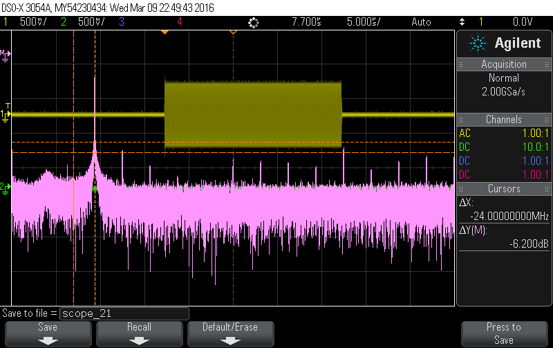
1) when i send constant 0x7ffffff0 (twos complement ), i can get a perfect sin waveform.

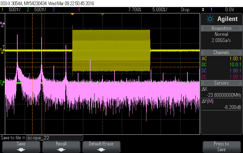
2) The data  i  send is :0x7ffffff0 - 50000*i . (twos complement ). the image2 attached is what i got from DAC output using oscilloscope.

     I think DAC output is out of order. Please help me to figure out what's the problem: DAC configuration errors or  DAC is broken

   Thank you so much and best regards


  • Hi Allen,

    It seems like you are using the DAC37J82 complex mixer. If you are using complex mixer, you must provide quadrature data.

    You will also need to initialze the complex mixer and NCO (if used) with the signal programmed in the 0x1F register. The easiest way is to program 0x1F register 0x8880, and then toggle the SIF_SYNC bit to 0x8882 to issue a initialization signal to the complex mixer.

    Please also include your setup description and GUI setting (snap-shots) so we can better help you.

    -Kang
  • Hi Kang,

    Thanks  for you reply. I'm not plan to use the  complex mixer and NCO,QMC. also they are disabled in my reg configuration. I use the SPI interface to configure DAC and my setup sequence is attached in the .txt file(reference document  0116.DAC38J84 Start-up Sequence.docx).

    my configuration : DAC37J82_4x_250MData_2lane_222mode_Fdac1000MHz_onchipPLLenable_inputclock1000MHz.
    please help me to check my registers configuration . Do these registers require any special consideration ?

    Thanks a lot .

    dac37j82_config_file.txt
    	// 1 set the DAC sleep pin to low
    
    	// 2 toggle the DAC RESETB pin to low and then high
    	
    	// 3 put JESD block in INIT state and reset jesd block
    	DAC_WriteReg(0x4A,0x003e);// bit0:0 reset jesd block bit4-bit1:1111 put JESD block into INIT_STATE
    
    	// set config 26,49,50,51 dac pll
    
    	// DAC PLL and OUTPUT sleep
    	DAC_WriteReg(0x1A,0x0003);// 0023 dac pll sleep
    	// dac pll settings
    	
    	////////////////////////////////////////////
    	DAC_WriteReg(0x31,0x0408);//n=1 lockdet_adj 000
    	DAC_WriteReg(0x32,0x0130);//m=1,p=5
    	///////////////////////////////////////////
    	DAC_WriteReg(0x33,0x4da8);//600uA charge current
    
    	// set config59,61,62  serdes pll
    
    	// serdes settings
    	DAC_WriteReg(0x3B,0x0800); //internal clock, div =1 means divide by 2
    	DAC_WriteReg(0x3C,0x0028);  // VRANGE =0 MPY=5
    
    	DAC_WriteReg(0x3D,0x0098);
     	DAC_WriteReg(0x3E,0x8128); //RATE:01(half)
    
    	// set config63,71,73,74,96
    	DAC_WriteReg(0x3F,0x00ff);
    	DAC_WriteReg(0x46,0x10c0);// lane 0 ID :2  lane1 ID:3  lane2 ID:0
    	DAC_WriteReg(0x47,0x090a);// lane 3 ID :1
    
    	DAC_WriteReg(0x48,0x31c3);
    	DAC_WriteReg(0x49,0x5550);
    	DAC_WriteReg(0x4A,0x033f);// put JESD block into INIT state and reset it
    
    	// set clkjesd_div,cdrvser_sysref_mode,interp registers
    		//jesd clock div
    	DAC_WriteReg(0x25,0x4000); 
    	DAC_WriteReg(0x24,0x20);
    	DAC_WriteReg(0x5c,0x02);
    
    	DAC_WriteReg(0x00,0x0218);//4x
    	
    	//verify pll lock by alarm_rw0_pll and alarm_rw1_pll
    	//  clear config108 alarms by write 0 to the register
    	DAC_WriteReg(0x6c,0x0);
    			// read cnofig108 make sure DAC PLL is locked and SERDES PLL locked
    		do{
    			 DAC_WriteReg(0x6c,0x0);
    
    			 data = DAC_ReadReg(0x6c);
    			 data = data & 0x0009;
    		}while(data !=0x0);
    	// set config3 ,config74-77,config79,80-85,config92,config97,
    
    
    	DAC_WriteReg(0x02,0x2002);
    
    
    	DAC_WriteReg(0x03,0xf300);
    	DAC_WriteReg(0x4A,0x033f);// put JESD block into INIT state and reset it
    		// JESD block settings
    		///////////////////////////////////
    	DAC_WriteReg(0x4B,0x1f01); //32 frame in multiframe configuration, 2 octets per frame per lane(222 configuration)
    	DAC_WriteReg(0x4C,0x1f01);
    	
    		////////////////////////////////////
    	DAC_WriteReg(0x4D,0x0100);
    	DAC_WriteReg(0x4E,0x0F0F);
    		//0x4f bit 5 no_lane_sync set1 to test CGS
    		//DAC_WriteReg(0x4F,0x1c61);// ILA ignored
    	DAC_WriteReg(0x4F,0x1cc1);//k28.0 1c
    
    		// sync request generate for link0
    	DAC_WriteReg(0x51,0x00dc);
    	DAC_WriteReg(0x52,0x00ff);
    
    		// sysref use all or one pulse skip
               DAC_WriteReg(0x5C,0x0002);
    
    	// alarms signal
    	DAC_WriteReg(0x04,0xFCFC);
    	DAC_WriteReg(0x05,0xEFF0);
    	// mask
    	DAC_WriteReg(0x06,0xFCFC);//fcfc
    	DAC_WriteReg(0x07,0x0000);
    	// DAC PLL and OUTPUT sleep
    	DAC_WriteReg(0x1A,0x0003);
    	// atest and alarm output
    	DAC_WriteReg(0x1B,0x1000);
    	// sync select
    	DAC_WriteReg(0x20,0x8008);
    	// path in select
    	DAC_WriteReg(0x22,0x1B1B);
    	DAC_WriteReg(0x23,0x01FF);
    	// octet path select
    	DAC_WriteReg(0x5F,0x0123);
    	DAC_WriteReg(0x60,0x4567);
    	// sync pin select
    	DAC_WriteReg(0x61,0x0010);// only sync_ab to fpga(link0)
    	// below are flag registers
    	DAC_WriteReg(0x2f,0x0004);
    	DAC_WriteReg(0x30,0x0);
    
    	//DAC_WriteReg(0x64,0x0000);
    	DAC_WriteReg(0x65,0x0000);
    	DAC_WriteReg(0x66,0x0000);
    	DAC_WriteReg(0x67,0x0000);
    	DAC_WriteReg(0x68,0x0000);
    	DAC_WriteReg(0x69,0x0000);
    	DAC_WriteReg(0x6A,0x0000);
    	DAC_WriteReg(0x6B,0x0000);
    	DAC_WriteReg(0x6C,0x0000);
    	DAC_WriteReg(0x6D,0x0000);
    	DAC_WriteReg(0x6E,0x0000);
    	DAC_WriteReg(0x6F,0x0000);
    	DAC_WriteReg(0x70,0x0000);
    	DAC_WriteReg(0x71,0x0000);
    	DAC_WriteReg(0x72,0x0000);
    	DAC_WriteReg(0x73,0x0000);
    	DAC_WriteReg(0x74,0x0000);
    	DAC_WriteReg(0x75,0x0000);
    	DAC_WriteReg(0x76,0x0000);
    	DAC_WriteReg(0x77,0x0000);
    	DAC_WriteReg(0x78,0x0000);
    	DAC_WriteReg(0x79,0x0000);
    	DAC_WriteReg(0x7A,0x0000);
    	DAC_WriteReg(0x7B,0x0000);
    	DAC_WriteReg(0x7C,0x0000);
    	DAC_WriteReg(0x7D,0x0000);
    	//   write config74 bit4-bit1 are all 0's (bring JESD out of INIT state)
     	DAC_WriteReg(0x4A,0x0320);
    
    	//  write config 74 bit0 to 1(bring JESD out of reset state)
     	DAC_WriteReg(0x4A,0x0321);


  • Hi Kang:

    1) As i described above, the data output to the DAC is generated by my NCO in FPGA. the mixer  and NCO is disabled in DAC.Then  we got the images attached above . when we use the mixer and NCO in DAC, we get the same result.(constant data input the DAC will get a perfect waveform, but liner data will out of order).

    2) I find my DAC registers configuration may be have one problem . I write 0x00dc in address 0x51, link configuration error(bit5 ) is ignored , because sometimes  this bit is 1 and will cause a sync request. I want to  know whether it can be ignored or not ?   Is this the reason why the DAC output out of order ?

  • Hi Kang:

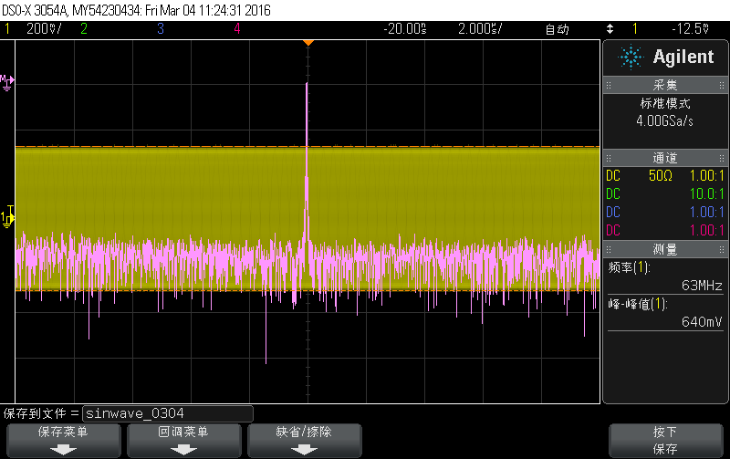
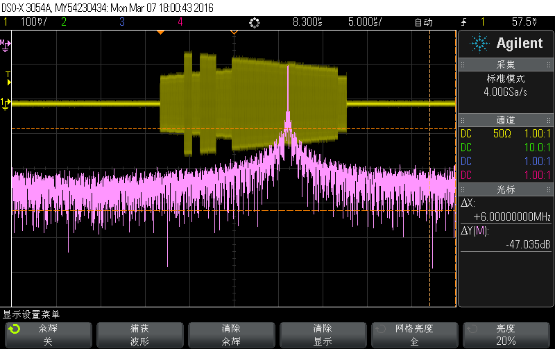
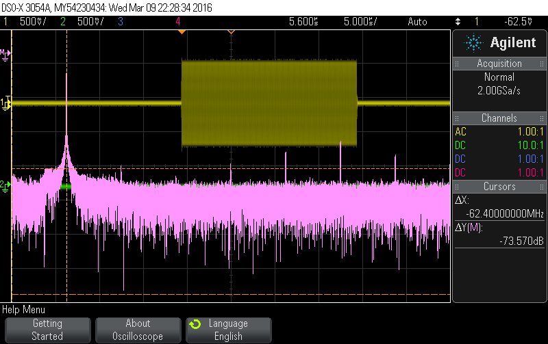
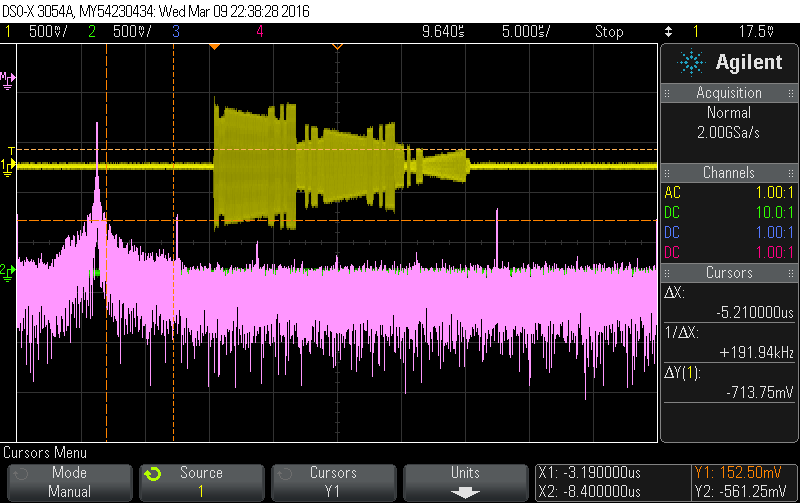
       the fiure below is the waveform i got from DAC output. 

    figure 1  62.5Mhz with constant value

    figure 2  62.5Mhz with  liner data(32768 -->  2678 )

    figure 3  31.25Mhz constant data -1

    figure 4  31.25Mhz constant data -2


    1 ) figure1and figure 2  : same frequency (62.5Mhz)with constant data  and liner data.

    2) figure 3 and figure4 : 31.25Mhz with constant data

    Q: we can get correct waveform when F=62.5Mhz. but  when using other frequency , we can't get correct waveform .  why?

  • Hi Allen,

    Can you please clarify what you mean by constant data? By constant data do you mean a sine wave(CW Signal) and linear data means the RAMP signal?

    Regards,
    Neeraj Gill
  • Hi Neeraj,
    Thanks for you reply.The constant and linear data are the amplitude of a sine wave. The sine wave is generated by NCO (inside or outside).
    best regards .
    Allen
  • Hi Allen,

    Since the DACs is able to generate a signal with constant amplitude I think the issue is with FPGA. Have you checked DACs output using DACs internal constant data? Please use DACs internal data and NCO to generate the signal at your desired frequencies.

    Regards,
    Neeraj Gill
  • Hi Neeraj,
    thanks for u help, the problem is solved. It's a configuration error, the SerDes lanes is inverted because config63 is set to 0xff. atfter i clearn this register. the output is normal.

    best regards
    Allen