This thread has been locked.

If you have a related question, please click the "Ask a related question" button in the top right corner. The newly created question will be automatically linked to this question.

Read DDR to file, DATA_READ_FAILED; Reset board DATA_READ_FAILED

Other Parts Discussed in Thread: ADC12J4000, LMK04828, CODELOADER

Hi,

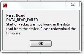
when I try to capture data from TSW14J56, it gives me this error:

then when I try to reset the board, it shows me this error:

I have also encountered Read DDR to file time out before.  So I want to know what are the reasons behind those errors?


My case is bit special since I'm using Avago optical to transmit my data, and try to capture it with my FPGA (if I connect ADC EVM and FPGA directly, there is not problem with capturing the data). But I just want to understand those errors, so I will know how to debug them.

There is only one documentation from Texas Instrument about setting up a JESD204B over optical, but the description in the document is very vague. I can't attach it here since it is confidential. But I'm certain someone from Texas Instrument knows how to configure this set up, since the set up from the document is exactly the same as mine. I just need some help to direct me to the right person so I can ask my other questions.

Thanks,

Angela

  • Angela,

    Can you provide some more info. What type of hardware is actually plugged into the TSW14J56? What is the JESD LMFS settings your are using? Is the K parameter the same on both sides? Is SYSREF and Device clock sent to the TSW14J56 using LVDS and at the correct frequency? All of these could cause the error you are seeing if not sent properly. 

    Regards,

    Jim

  • I'm loading ADC12J4000 Bypass firmware into TSW14J56

    What type of hardware is actually plugged into the TSW14J56?

    the hardware that is plugged into TSW14J56 is LMK04828 EVM.

    What is the JESD LMFS settings your are using?

    The JESD LMFS settings are L = 8, F = 8, K = 4

    Is the K parameter the same on both sides?

    I think so, since I didn't change K parameters

    Is SYSREF and Device clock sent to the TSW14J56 using LVDS and at the correct frequency?

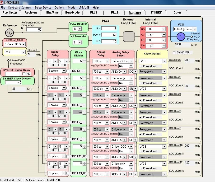
    yes, the SYSREF is 25MHz, there are two pairs of device clock sent to TSW14J56(DCLK0 and DCLK10 in my case) both at 200MHz

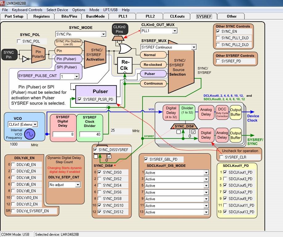
    I have noticed that my DCLK0 doesn't output correct frequency above 125MHz, so it never outputs 200MHz to TSW14J56 even I set everything correctly. DCLK10 is able to output 200MHz without any problem, but both my settings for those to clock outputs are exactly the same. So I suspect if the DCLK0 hasn't synced with other clock outputs correctly? I have followed the attachment below to establish my SYSREF and SYNC. My question is :

    1. what could be the reason that only my DCLK0 doesn't output correct frequency above 126MHz, but the rest of my clock outputs are fine?

    2.how do I know what value to set device clock, SYSREF divider and SYSREF clock digital delays?

    3. what is device clock digital delay half step? and what value should I set them?

    4. Do you think those digital delays are relevant to my problem?

    5. if my DCLK0 analog delay select is divider only, the LVDS signals are not at same voltage level, hence VDCLK0 is between 0.9V and 1.3V with Vp-p around 300mV but VDCLK0* is between 1.4V and 1.6V with Vp-p around 150mV, so the differential signals negative and positive don't even overlap, which I found very strange. But once I change the analog delay select to divider + DCC+ HS, then the voltage level are the same. There is not effect to DCLK10, whether I choose analog delay select for divider +DCC+HS or divider only. Could you tell me what can be the possible reason?

    I also attached my CodeLoader GUI so you can take a look over my settings

    Key Points to setting up SYSREF on LMK0482x_e2e_2016-06-29.pdf

  • Angela,

    For #1, contact the LMK clock group to find out if there is an issue with their GUI and or EVM regarding this.

    For #2, Use the attached file to help with calculating SYSREF. In HSDC Pro GUI, after you load firmware and enter the ADC output data rate, a window will open showing what device clock frequency needs to be sent the TSW14J56.

    For #3, normally not used. For all LMK settings you are confused about, run the ADC GUI and observe all of the register settings after the configuration file has been loaded or go the ADC GUI configuration folder and look at the configuration files directly for register settings. Any register not written to will use the default power up value.

    For #4, no.

    For #5, see answer to #1.

    Regards,

    Jim

    Calculating SYSREF.pptx

  • Do you have contact information for LMK clock group?
  • Clock and Timing Forum on E2E
  • Hi Jim,

    Now that I have figured out my questions with LMK04828, I'm still not able to capture the data. Every time when I capture it shows me read DDR to file time out error, and I suspect it's the JESD configuration are not matching, do you know how can I check?

    Thanks
    Angela
  • Angela,

    Try to capture the data using our ADC board setup with the parameters you are using for your custom optical ADC interface. This may help figure out what parameter might be wrong. What LMFS setting would this be? What lane rate are you expecting?

    Regards,

    Jim

  • Hi Jim,

    I have already tried to capture the waveform and compared it with ADC EVM, and all the signals seem correct. Can I email you or send to your inbox the document that I want to show you? I think this document might help you explain what I'm trying to do, but since it's confidential by TI, so I don't think I should share it here.

    Thank you
    Angela