This thread has been locked.

If you have a related question, please click the "Ask a related question" button in the top right corner. The newly created question will be automatically linked to this question.

ADS5500 Input Protection

Other Parts Discussed in Thread: THS4500, ADS5500, LMH6553, ADS5500-EP, THS4500-EP

Hi,

We are driving ADS5500 using ADC driver THS4500. The Driver operates with +/-5V supply. This is higher than the rated ADC analog input voltage.

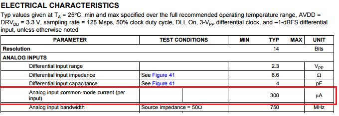
Can you suggest the suitable input Protection to prevent damage to ADC? We tried using Clamp diode, but we are having a 250 ohm diode current limiting resistor. The datasheet mentions the ADC has input Common mode current of 2ma through each pin. This current causes almost 0.5V drop across 250 ohm resistor, hence we will not meet input range of ADC.

Can you suggest appropriate protection scheme?

Regards,

Veerasamy

  • Veerasamy,

    We are looking into this.

    Regards,

    Jim

  • Hi Vasudevan,

    Have you looked at the LMH6553 as using an ADC driver? This part has an integrated output clamp that allows output signal swing control while driving the ADC inputs. It is available in an 8-pin SOIC package as well, similar to the THS4500 and should be easily replaceable because it is pin-to-pin compatible (except that the LMH6553 has a clamp pin instead of the THS4500 PD pin). 

    If you still intend to use external ADC input protection, then I feel that using clamp diodes should be the best option. However, if I look through the ADC datasheet, the ADC input common mode current is specified around 300uA through each pin, which will only amount to 75mV through the 250 ohm resistor. So, there is some disconnect which I am not able to understand. Would it be possible for you to attach your schematic here?

    Best Regards,

    Rohit 

  • Hi,

    Thanks for suggesting LMH6553. But we are looking for Extended Range parts. (-EP). Please find Common Mode current from datasheet. The current is mentioned as 4mA

  • Sorry Image not pasted. Please look into datasheet of ADS5500-EP. Page - 5
  • Hi Veerasamy,

    I understand. But, I think during normal operation, the clamp diode should be reverse biased or turned off. This means that minimal reverse bias current should flow through the 250ohm resistor protection resistors and thus, you should see minimal voltage drop. I don't think the 4mA of total analog input common mode current should come into picture with the clamp diodes in normal operation, because the clamp diode path is high impedance. It might be helpful if you could attach your schematic to help debug further.

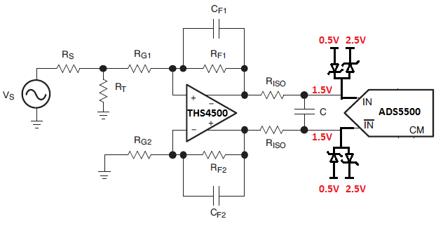
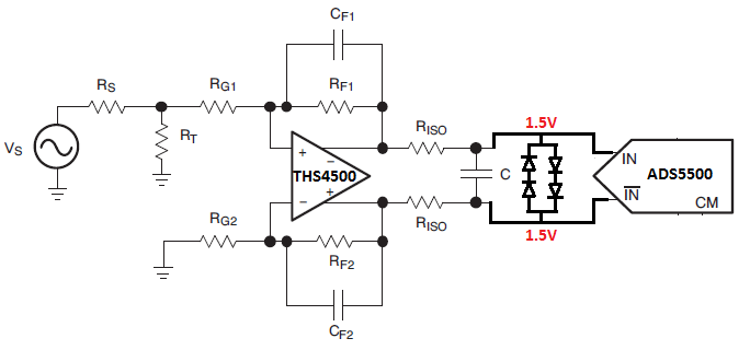
    I think you can use either of the below two protection schemes between the THS4500-EP and the ADS5500-EP, one using Schottky diodes and the other using TVS (transient voltage stabilizer) diodes. For the schottky diode approach, I would recommend using a Schottky diode with 2V breakdown voltage like the SBX201C from On-Semi for overvoltage detection beyond 2.5V. I would also recommend the TVS diodes to be within 2V breakdown voltage like the uClamp2511T from Semtech.

    Best Regards,

    Rohit

    1. Using Schottky diodes:

    2. Using TVS diodes:

  • Hi,

    Thanks for Reply. Sorry we do not have any schematics at the moment. However the design is same as your circuit shown above (Schottky diode solution). Riso will also function as current limiting to Clamp diodes. Its value is 250 ohms. So the 4mA common mode current should go through Riso and cause significant drop right. This 4mA will flow through this resistor independent of whether the diode is in Normal operation or in Clamp mode.

    Regards,

    Veerasamy

  • Hi Veerasamy,

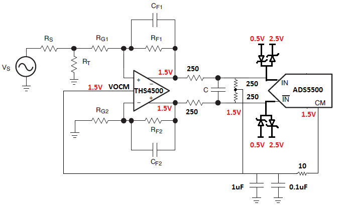
    You could use a center tap resistor divider at the ADC inputs tied to its VCM in-order to not have this voltage drop due to the 4mA common mode current. Also, you would need to connect the output common mode voltage of THS4500 to the ADC VCM output, as shown below.

    Now, the differential signal will be reduced by 6dB which I think you should be okay given that the amplifier signal swing is much higher than the ADC full scale input signal swing. You could also increase the value of center tap resistors if lesser voltage loss is desired.

    Best Regards,

    Rohit

  • Hi,

    Thanks a lot. This is very helpful.