This thread has been locked.

If you have a related question, please click the "Ask a related question" button in the top right corner. The newly created question will be automatically linked to this question.

Calibration of ADC07D1520 and DC-bias of the analog I/Q inputs

Other Parts Discussed in Thread: ADC07D1520

Hi,

This may seem like an odd question, but could help explain some odd behavior of custom ADC boards we are debugging:


We are using DC-coupled signals to the I/Q inputs.

Will the ADC07D1520 undergo a power or user-initiated calibration cycle if the common-mode bias of the LVDS I/Q inputs is 500 mV larger or smaller than the 1.25V internal Vcmo of the ADC chip?


Will the data clock output be operational in this case as well?


I understand this situation is non-optimal for the ADC chip, and we're trying to figure out why the unity-gain buffer from the Vcmo ADC pin is not working correctly, but in the meantime any advice would be great.

Thanks,

Eric

  • Hi Eric

    The ADC07D1520 input CLK+/- must be AC-coupled to allow the device to set the input common mode and optimize the duty cycle for DES modes of operation.

    For the analog inputs, driving a signal with a common mode voltage that is significantly lower or higher than the Vcmo voltage will result in degraded harmonic performance. To achieve rated performance the common mode input voltage on I+/- and Q+/- must be within 50mV of the Vcmo output voltage.

    The improper common mode input voltage will not cause the device to initiate a calibration. Re-calibrating the device will not provide rated performance until the input common mode is within specifications.

    Best regards,

    Jim B

  • Hi Jim,
    Thanks for the reply. Yes, our CLk+/- is AC coupled and of an appropriate amplitude.

    Is there anything that would *prevent* a calibration from running (i.e. high signal on the CalRun pin)? With PD low and the chip in non-ECE mode, the ADC is unresponsive to an appropriate-length pulse at the CAL pin. The ADC is also not outputting a data clock.

    There is most likely something wrong in our system, but I'm asking in case these issues point to a certain failure or hardware error you may be familiar with.

    appreciated,
    Eric
  • Hi Eric

    If the device is in non-ECE mode the following can prevent calibration from running.

    • PD pin not pulled to GND, so device is in PowerDown mode.
    • PDQ pin not pulled to GND so Q channel is in PowerDown mode. This will prevent the Q channel only from calibrating.


    If the device is in ECE mode, having the CAL bit set high can prevent calibration from working. This is because the CAL pin and CAL bit are internally OR'd and the calibration is started after a positive pulse on the internal CAL request signal.

    Please note: There is a combination of pin control settings (of pins 52 and 14) that can enable ECE mode even if Pin 41 (ECEb) is high. Can you share a schematic snapshot showing the ccty around the ADC including the logic level at all input control pins?

    Best regards,

    Jim B

  • Hi Jim,

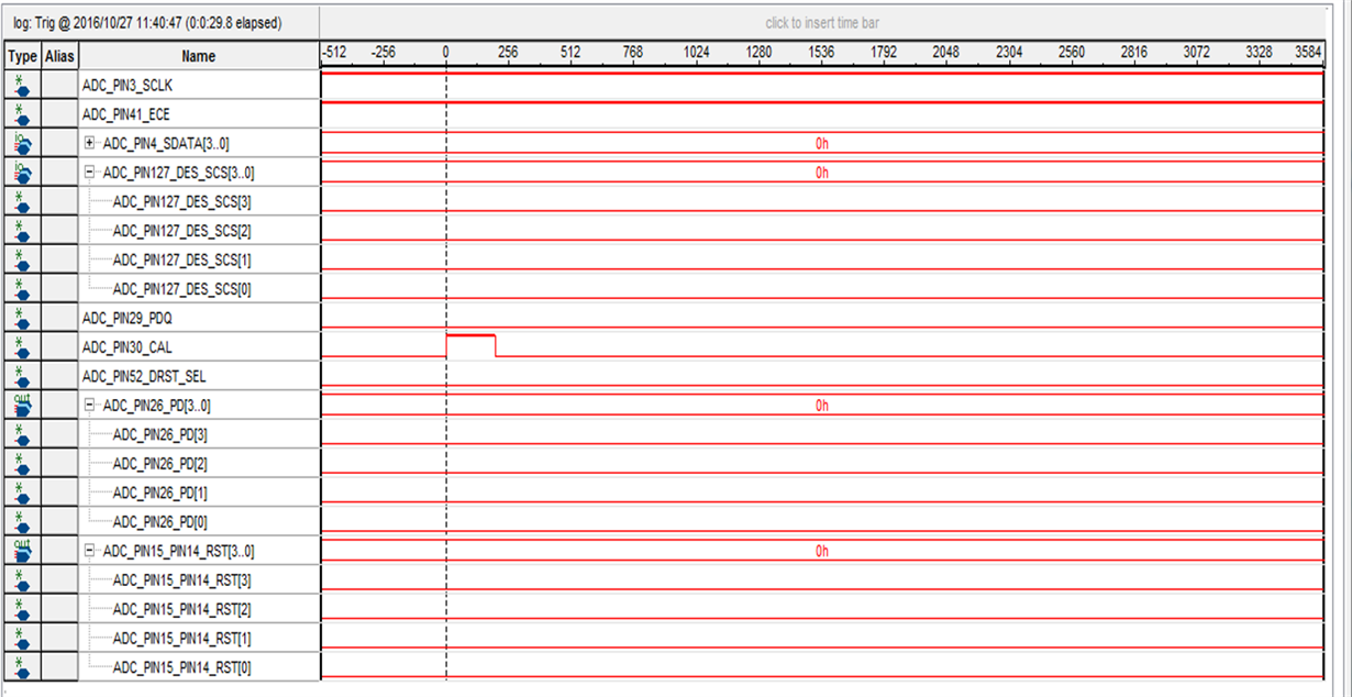
    Here is a snapshot of all the logic levels of the ADC control lines, including a cal pulse signal. The x-scale units are microseconds. A few of the signals are bussed since our design includes four ADC07D1520's. DCLK_RST is used in differential mode.

    A schematic of the ADC and front-end block can be found here:

    2868_Sheet_12_1.pdf

    I appreciate your time!

    Eric

  • Hi Jim,
    I may have fixed this: we mistakenly flipped the LVDS pairs in the DCLK_RST signal. So this signal was being held high all the time.

    By fixing the LVDS polarity, I can now see the calibration cycle active via CALRUN and a data clock on DCLK+/-. Have not verified the data stream yet, but the ADC activity looks much more promising now.

    I don't recall reading in the datasheet where holding DCLK_RST high would prevent the chip from calibrating, hence this mystery. Maybe I missed this.

    thanks,
    Eric
  • Hi Eric

    That's good news!

    When DCLK_RST is asserted it is basically holding the internal CLK/4 divider circuitry in a reset state. In that condition most of the internal digital processes are inactive including data output, calibration etc.

    Best regards,

    Jim B