This thread has been locked.

If you have a related question, please click the "Ask a related question" button in the top right corner. The newly created question will be automatically linked to this question.

ADS54J54: Difficulty getting code group synchronization and initial lane assignment.

Part Number: ADS54J54
Other Parts Discussed in Thread: LMK04828

I'm using the ADS54J54  in conjunction with the LMK0428 clock jitter cleaner and am observing strange behavior from the ADC.  The LMK0428 is providing 500 MHz clocks, as well as the SYSREF input to the ADC.  I am using a pulse/one shot method for SYSREF, which was recommended by the datasheet.

Here's my steps and results:

I program the ADS54J54 using the following steps from the datasheet:

7.3.12 JESD204B Interface Initialization Sequence
After power-up, the internal JESD204B digital block must be initialized with the following sequence of steps:

1. Set JESD RESET AB/CD and JESD INIT AB/CD to 0 (address 0x0D, value 0x0000)
2. Set JESD INIT AB/CD to 1 (0x0D, 0x0202)
3. Set JESD RESET AB/CD to 1 (0x0D, 0x0303)
4. Configure all other JESD register and clock settings. If those settings change later on, this initialization
sequence must be repeated.
5. Set JESD RESET AB/CD to 0 (0x0D, 0x0202)
6. Set JESD RESET AB/CD to 1 (0x0D, 0x0303)
7. Wait for two SYSREF pulses
8. Set JESD INIT AB/CD to 0 (0x0D, 0x0101)

After step 8, the device immediately starts sending K-characters.   This is not expected.  According to the data sheet, I shouldn't receive K-characters until SYSREF is asserted followed by a SYNC.    See the figure below.   If I assert SYSREF, then the k-characters stop momentarily, and other characters are transmitted, but they aren't consistent with the ILA process.  After a few dozen random characters are received, the received data returns to being k-characters indefinitely.    

Oddly, SYNC, doesn't seem to have any affect on the ADCs behavior.  

Thanks in advance for your help.


  • Hi,

    is this on your own hardware rather than the EVM?  I have not seen such behavior with our EVM into the TSW14J56 FPGA card we have, but I have not had to look at what was coming right out of the ADC since it would sync up a JESD204b link with the FPGA.     I have to ask though, are you controlling the SYNC input that goes to the channels you are looking at?  There are two SYNC inputs to the device, one for channels A and B, and the other for channels C and D.   Our FPGA firmware for the TSW14J56 drives two SYNC signals to the FMC connector to route through to the ADC.

    Much of what is in the config files for the EVM and TSW14J56 involves setting up the LMK and most of the writes to the ADC are the steps in that section 7.3.12 you call out.  and then some trim adjustment for the ADC.  It looks like I didn't worry too much about getting step 4 done precisely at that point in the sequence, or make step 7 wait on anything.  The SPI writes from the PC running the GUI are slow enough that step 7 could not happen too fast.  And I have different config files for the different LMFS modes of operation so I don't switch around between different modes without also doing the re-init step.   But I do have the LMK all set up before I go though the ADC config.  Config file that I use is attached, just for reference.

    I may need to get a list of just what register writes you are doing and then check it over, compare to what we do, or try your config in our setup.

    Regards,

    Richard P.

  • Thanks Richard,

    I don't see the attachment of the config file. Did you forget to attach it, or am I just missing something? I'm eager to see what steps you are doing to program the part.

    I am using my own hardware, which is an FPGA. The FPGA drives the SYNC inputs on the ADC. I'm actually viewing the received data using an internal logic analyzer inside the FPGA. (It's where I'm seeing the K-characters).

    I set up the LMK prior to configuring the ADC.

    Step 4 that I listed is vague. It's not clear what registers are specific to "JESD register and clock settings." So I literally program all of the registers in this step.

    One item that is not clear to me is how sysref should be configured. The data sheet says in section 7.3.4 that for a one shot strategy, says
    "A single SYSREF reset pulse is used to synchronize the ADS54J54. The ADS54J54 device requires a minimum of 3 SYSREF pulses to complete the synchronization phase." So do I need a single pulse, or multiple pulses? How wide should the pulses be? This information is critical to programming the LMK to generate a good sysref.

    I'm happy to send you my programming file to show you my steps.

    Thanks for your help.
  • Hi,

    Yes, I forgot to attach the attachment.  My apologies.  Here it is.  In my more recent EVMs I have been programming the LMK to set up clocks and SYSREF and then programming the ADC, and then at the end going back to program the SYSREF to be turned off for the ADC but still running for the FPGA.   We get some coupling between clock and SYSREF the gives rise to some spurs in the resulting FFT if SYSREF is continuously running.  Thus we recommend turning off SYSREF.    But maybe here for development purposes we should leave SYSREF running continuously until we get everything up and running and stable.   Then we could go back and insert into the configuration to turn off SYSREF when no longer needed.    The only harm a continuous SYSREF should present during development is a minor degradation in AC performance (some low level spurs in the spectrum.)

    But as you can see in this config file I just configure the LMK first and then the ADC.  After the main section programming the LMK there is another section of LMK programming that has to do with specifically SYSREF, and then the ADC configuration.  I didn't write that second section of LMK config that deals with setting up and triggering the SYSREF.  If need be I can consult with the person who did write that portion when he is back in office next week. 

    I believe there needs to be some number of SYSREF pulses before it can be turned off.  I do not know the minimum number.   There is no requirement on the duty cycle of SYSREF as only the rising edge of SYSREF is detected and used.  But the frequency of SYSREF is crucial.  Once you set up a mode of operation with a specific LMFS setting, and then pick a value for K, you have chosen the size of a MultiFrame of data.   SYSREF edges must be exactly on the boundaries of these Multiframes.  So there is a divider value in the LMK that is set for setting the SYSREF frequency.  If I remember right, there are two different LMFS modes possible for this ADC - one with 8 lanes and one with 4 lanes.  I think we set up the config of the LMK with a certain SYSREF divider value, and then in the config of the ADC for 8 lane mode we had a K value that worked with that SYSREF divider value and in the 4 lane mode we had a different K value that also worked with that same SYSREF divider value.  

    Regards,

    Richard P.

    ADS54J54_500M_841.cfg

  • Richard,

    I focused today solely on working on the LMK part to get a SYSREF going on my hardware.  I did get it to work, but I have a few comments/questions.  The sysref-centric lines of code in your config file are lines 111-123, which I have copied below:

    111    0x139 0x00 //set SYSREF_Mux to "Normal"
    112    0x143 0x11 //set SYNC_MUX to "Pin"
    113    0x140 0x00 //turn on all the blocks, can these just stay on?
    114    0x144 0x74 //enable syncing of all clock outputs
    115    0x143 0x11 //trigger SYNC event using "Pin" mode
    116    0x143 0x31
    117    0x143 0x11
    118    0x144 0xFF //disable syncing of all clock outputs
    119    0x139 0x3 //set SYSREF_MUX to "Continuous"
    120    0x13E 0x3 //set SYSREF pulses to "8"
    121    0x143 0x12 //trigger SYNC event using "Pin (Pulser)" mode
    122   0x143 0x32
    123   0x143 0x12

    I found that lines 111-117 generate a long, single SYSREF that is manually triggered.  Lines 118 to 123 generate a continuous SYSREF.  Is this the intent?   What was confusing was that several lines of code here are not necessary and are misleading  lines 119-123 don't have any affect on the LMK, since it has been placed into continuous mode in line 119.  

    I'm going to try out programming the ADC shortly.  

  • Richard,

    I was able to get the ADC programmed and have had some success. I've been running some test patterns and could use some additional help.

    I'm using LMFS = 8411 and am observing the received data on both lanes using the test patterns from the ADC. The test pattern for alternating data looks good across both lanes. However, the ramp pattern is puzzling. The lane that transmits the least significant byte is correct. It ramps up and down smoothly. The most significant byte lane has some semblance of a pattern, but it is not a ramp. Could I be missing something with the programming of the ADC?

    Thanks for your support.
  • Hi,

    I spoke with the person who generated some of the first config files for the EVMs using the LMK04828 with our JESD204b dataconverters, and that section of LMK configuration in lines 111 to 123 were something that he had gotten from some discussion of the LMK configuration, possibly in the clocking forum.  At any rate, what that section is doing is first allowing a SYNC event to reset the counters for the SYSREF counter and the clock dividers that are actually being used for the ADC and the FPGA, and then causing a trigger event to reset the counters to synchronize them.   Then the sync event is masked and a trigger event issued for the SYSREF itself.  it is address x144 that is used first to enable some of the counters to be sync'd.  (The comment says enable all outputs to be sync'd but when I look at the value x74 only some are enabled - the ones that are used in our design)  Then that same address gets x144 to disable any further synchronizing of the counters.    we got this block of code from the LMK people, so I suggest the clocking forum might be better for closer examination of what is going on there.

    I have not seen an issue with ramp on my checkout of the EVM,  Might a see a screenshot of what you are seeing on the most significant byte that doesn't look right?  I can't think of anything that would mess up only one byte of the pattern, unless is it the selection of offsetbinary vs two's complement, and that would only result in the most significant bit of the pattern being inverted.

    Regards,

    Richard P.

  • Richard,

    Today I worked on the ramp test pattern, and observed similar results as yesterday, albeit it's a little bit better.  I experimented with two different lanes on the device to see if their were any differences.  The other lanes acted exactly the same.  The least significant byte is perfect and shows a nice incrementing pattern. The most significant byte looks good for several hundred samples, but then goes wacky.  I've attached an excel file that shows my results, which were captured via an internal logic analyzer in an FPGA.  

    Column A gives the sample number as a reference.  It starts on 146 because the samples before that are not meaningful because of initialization.

    Column B is the data observed for lane 1, which looks good for the entire sampling time.

    Column C is the data observed for lane 0, it looks good until about sample number 320.  The pattern is not random, but certainly no longer resembles a counting pattern.

    I just tried to insert a file using the RTF editor. Hopefully you can download it.  If this doesn't work right, please give me guidance on how to upload a file.   Otherwise, I can paste the file here -- it's not terribly long.

     iladata_2.xlsx

  • Hi,

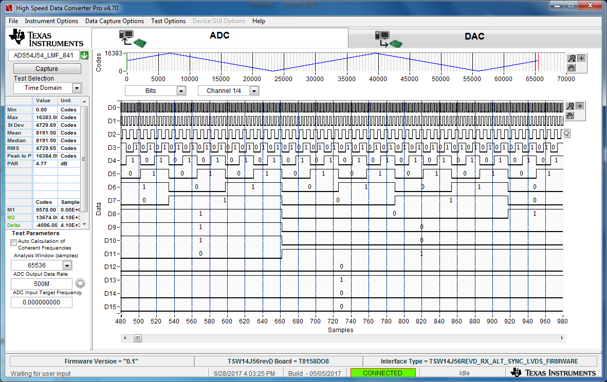
    I just powered up my EVM into our TSW14J56 and flipped back and forth between normal and ramp for channels A,B and for channels C,D.  I do see the ramp pattern as normal on each of the channels.  Please see the screenshot for one of the channels.  I did have to invert the most significant bit of the sample to make my capture card software happy, as it was expecting either offset binary of two's complement while the EVM was outputting the opposite.  But it is still a recognizable ramp with the msb inverted.  My first suspicion would be the bits coming off your FPGA IP are not quite in the order you are expecting to see and the data being scrambled up in some order, but that would just be a  guess.   if there were a setting off in the LMFS and K parameters somewhere then I would expect the FPGA to have trouble with the ILA after SYNC.

    Regards,

    Richard P

  • Thanks for the update. It is puzzling why the ADC is behaving this way. My values for LMFS are correct....I've double checked them....and I consistently get ILAS sync. I can't figure out why one lane works and the other doesn't. I've examined one of the other converters of the device and the results are identical.

    Since this is a 14 bit ADC, are D14 and D15 logic zero in your setup? I have noticed that the two LSBs are zero when I receive the raw data, which is consistent with the data sheet. This includes the two LSBs for the alternating pattern.

    Perhaps I'm programming the device in the wrong order. Right now I do the initialization sequence from your script. Then I turn on the ramp pattern, and then I issue a sync_n. Maybe I need to program the ramp pattern during the initialization process?
  • Hi,

    Looking at how the data is parsed after it comes out of the TSW14J56 FPGA IP it agrees with the data sheet that the 14 bits are msb-justified with two zeros appended at the end.  The table 3 in the datasheet lists bits 13:6 and then 5:0 plus two zeros and that is what I see.   The TSW14J56 just takes a block of data from the FPGA JESD204b IP for the 8 lanes and loads that into memory just as it comes from the JESD block.  Then that data has to be parsed into samples and that is listed in the ini file for the device in the HSDCPro folders.  For LMFS 8411 I see:

    Bit Packing Channel Pattern=C1S1[13:6],C1S2[13:6],C1S3[13:6],C1S4[13:6],C1S1[5:0],T[2],C1S2[5:0],T[2],C1S3[5:0],T[2],C1S4[5:0],T[2],C2S1[13:6],C2S2[13:6],C2S3[13:6],C2S4[13:6],C2S1[5:0],T[2],C2S2[5:0],T[2],C2S3[5:0],T[2],C2S4[5:0],T[2],C3S1[13:6],C3S2[13:6],C3S3[13:6],C3S4[13:6],C3S1[5:0],T[2],C3S2[5:0],T[2],C3S3[5:0],T[2],C3S4[5:0],T[2],C4S1[13:6],C4S2[13:6],C4S3[13:6],C4S4[13:6],C4S1[5:0],T[2],C4S2[5:0],T[2],C4S3[5:0],T[2],C4S4[5:0],T[2]

    That is a long string of stuff to pick through but that is what we have to create to get the bits in the right places.   This string of data says that of the first chunk of 32 bits that was pushed into the RAM it contained the top 8 bits of channel1, sample1, then channel1, sample2, then channel1,sample3 and channel1,sample4.   Then the next chuck of 32 bits contained the lower 6 bits of these same samples plus two tail bits of zero.   Then the same thing for channel2.  then the same thing for channel3.  finally the same thing for channel4.    This was for 8 lane mode, so what was pushed into memory was 32 bits of the first lane, then 32bits of the second lane, then 32 bits off the third lane, 32bits off the fourth lane, and so on for all 8 lanes.     Then the above string was used to pick apart what bits went where.  Actually, that aligns with a frame of data from table3 exactly.   I am thinking something in your code is having to do a similar thing but doesn't quite have all the bits going the right places.  This is all after the ILA is handled by the IP.   The JESD IP handles the ILA directly and then hands off the data from the IP block to the FPGA fabric to process.  Since your FPGA seems to be handling the ILA okay, but scrambling the data after that, that is the reason I think the data is being misprocessed after the JESD IP block.   Also, the LMFS parameters should all be correct since the IP block doesn't have a problem with the ILA. 

    It is at a time like this that I wish the ADC has a test pattern option to set a custom pattern.  Many of our other ADCs do.  That lets me set the test pattern to 00 0000 0000 0001 and send that data pattern.  then I look at the captured data to see where that single '1' landed.  Then I walk that '1' by one position to 00 0000 0000 0010 and repeat.    That way I can map out the pattern of what bits are where at the end of the chain.  I don't see that as an option here unfortunately.

    Also, all I did was load the default config file for the 8 lane mode, and then click on the GUI control bits for the test patterns.  I did not have to weave the test pattern setup in with the config file.   I just configured the LMK and ADC and then went back to set the test pattern bits.

    Regards,

    Richard P.