This thread has been locked.

If you have a related question, please click the "Ask a related question" button in the top right corner. The newly created question will be automatically linked to this question.

ADC31JB68: K28.5 data not always sent after power-up, when sync is low

Part Number: ADC31JB68

We've got the ADC31JB68 connected to a Xilinx Artix-7 FPGA, and are using the giga-bit transceiver GTP IP to interface to it.

The problem is when sync is driven low after power-up. K28.5 data is expected on both lanes (xBC seen on the parallel data output of the Xilinx IP). Sometimes both lanes send this data and when sync is driven high, correct captured data can be seen. The interface will always behave correctly from here. However on other occasions neither or only one of the lanes transmits K28.5, and no combination of resets or re-syncs seem to change this. Reloading the FPGA image will change the lanes that output correct K28.5 data.

It would appear that there is some kind of power-up or data alignment issue.

  • Hi Andrew,

    I am looking into this issue, and will get back with you soon.

    Are you using the ADC31JB68EVM? Can you please provide the register settings that you are writing to the ADC?

    Regards,

    Dan
  • We're not using the evaluation board, this is our own custom design.

    All register values are as power on default.
  • Hi Andrew

    Can you provide the following information?

    • ADC CLKIN frequency
    • ADC SYSREF status/frequency. Is the ADC SYSREF active or static?
    • FPGA SYSREF frequency
    • FPGA CLK frequencies

    Is the ADC stable and being clocked when the FPGA IP is loaded and enabled?

    In my experience it is best to have the ADC JESD204B interface ready to go before enabling the FPGA IP.

    Best regards,

    Jim B

  • We intend to run this at 500M eventually, but I have slowed down the clocks during debug.

    - ADC clkin = 100M

    - sysref is static and unused

    - Frequencies used in FPGA rx are 100M, and 25M

    During debug, the board is powered up, and then the FPGA is configured from the PC using JTAG. The following pins are driven the same, before and after FPGA config:

    - syncb- = 1.6V

    - syncb+ = 0.2V

    - clkin- = 100M

    - clkin+ = 100M

    so the ADCs should be running before their serial data is sampled.

    I've also noticed that if a lane doesn't send K28.5 after power-up, then it will also not send this data if K28.5 test mode is selected.

    I suspect that the issue might be caused by the Xilinx GTP IP not correctly framing the serial data when it fires up. It has an optional pin called RXSLIDE, which allows the receiver to perform manual alignment. I'll try driving this to see if I can get the correct data to appear.

  • The slide function improves the situation, but still does not provide a solution where K28.5 can always be seen on all lanes.
  • Hi Andrew

    I'm not sure what might be causing the issues you are experiencing.

    Can you share the schematic for all ADC related circuitry so I can review that information?

    Can you use the Xilinx JESD204B IP to look at the signal quality (data eye) on the RX lanes of the FPGA?

    Best regards,

    Jim B

  • ADC schematic is shown above. We have 4 ADCs connected to two 4 lane GTP IPs in the Xilinx FPGA.

    We have a second (identical) board which seems to behaving correctly. The issue on the first board appears to be due to the FPGA configuration. After the image is loaded for the first time, the GTP IP does not assert any reset done outputs. When it is loaded for a second time the IP comes out of reset, but with indeterminate K28.5 values.

    I'll try to extract the eye diagram info from the FPGA.

  • Hi Andrew

    I don't see anything obviously wrong on the schematic. I do have a question about where the GND_CHn to GND star point connectors are placed? This needs to be done so that the JESD204B data buses aren't routed over any gaps between GND planes.

    If you see good results on one board, and the good versus bad lanes seem to change from FPGA config to config, then I would be investigate the power supply rails for the FPGA on the problem board. I have seen issues where incorrect voltage levels, or noise on the supplies has caused symptoms similar to what you are encountering. I would start with the power buses specific to the transceivers used for the ADCs in question.

    Best regards,

    Jim B

  • Thanks for the information. I'll bear it all in mind when I return to debugging the second board, and hopefully be able to give some feedback.

  • The issue seems to have been a problem with the Xilinx IP during initialisation. The IP needs a clock to be running during initialisation and reset.

    We have another problem with the digital range. There are sine waves on the inputs to Vin+ and Vin- with peaks at approx 1.6V +/- 0.1V. This gives a digital range of approx 0900 to F700.
    However when the sine wave amplitude is increased much above 0.1V the digital output becomes totally spurious.

  • Hi Andrew

    Can you provide text files showing the exported ADC data for both cases?

    If you are going beyond full-scale I do expect to see significant distortion increase, but that shouldn't be the case if the signal is still below full scale limits.

    Best regards,

    Jim B

  • I have dumps of the data below. Ignore the alternate columns of FFFFFF. The input is a 1 MHz sine wave (we're sampling at 200M).

    This is for input of approx. 1.6V +/- 0.1V:

    This is when the input is increased by approx. 10%:

  • Hi Andrew
    I'm not sure what is causing the change in data output as you increase the input amplitude.
    I would recommend using Ramp Test Pattern (see JESD_CTRL2) to confirm proper data transfer and post-processing. If that is OK then you can proceed to debug other possible causes of the distortion.
    Best regards,
    Jim B
  • I've placed both lanes of the ADC into ramp test mode and can see the correct, full-scale digital range being generated and processed.

    The problem would seem to be in the analogue capture. Do you have any recommendations of where to start looking?

  • Hi Andrew
    Initial things to check are that the input signal meets the input common mode voltage and differential amplitude requirements of the ADC. If the common mode is not correct that can cause problems.
    See Driving the Analog Input in the datasheet for more details regarding proper input drive techniques.
  • The voltages and signals on the pins of the ADC all look correct. We're not driving the sysref inputs, with the gate being disabled by default.

    When miso is configured to act as an overflow, it never gets driven high.
  • Hi Andrew

    I'm still trying to come up with a theory of what is happening.

    For your data capture that does seem to be working, you say the signal level is 1.6V +/- 0.1V.

    Is that 1.6V peak to peak at the 50 ohm input to the transformers? or 1.6V peak to peak differential at the ADC inputs? Or something else?

    Can you confirm the clock frequency is 200 MHz and CLKDIV = 1?

    I did notice that the baluns used are only rated for 4.5 MHz to 3000 MHz operation. Can you try increasing the frequency to 10 or 20 MHz to see if the behavior changes?

    Best regards,

    Jim B

  • I'm measuring the voltages at the pins on the ADC. Approx voltages are:

    VCM = 1.6V

    VIN+/VIN- = SIne waves centred on 1.6V, with peaks of 1.5V and 1.7V, ie sine wave amplitude of 0.1V with 1.6V offset.

    Clock frequency is 200M, and OM2 register is left as default.

    Changing the frequency to 10M doesn't change the behaviour.

  • I've been looking at received data on the high byte lane after sync is pulsed low. The ILA sequence is seen, followed by the sampled data. This looks correct for the first few samples (can be anything between a few and a few hundred). Then the data becomes spurious. I've tried sine waves of up to 1V peak to peak, and the initial data seems OK.

  • On further analysis, I have found that by reducing the sample rate to 100M, the behaviour seems correct, and I can continuously get full digital range.
  • Hi Andrew
    Given the ADC data looks correct with ramp test mode at 200 MSPS but only captures properly at 100MSPS I'm wondering if there could be any issues with the power supplies at higher clock rates when the analog input is present.
    Can you measure the DC voltage and ripple on all power supplies in both ramp test mode and in normal operation with no input and with a larger input applied?
    It would also be worth verifying the FPGA power supplies are all within spec under the different conditions (before configuration, after configuration, link operating at 1 Gbit/sec, link operating at 2 Gbit/sec, with test pattern and real ADC signals, etc.
    Regards,
    Jim B
  • I've investigated the voltages on the power rails to the ADCs and FPGA. To minimise noise and ripple, I powered the board from a lab DC power supply, which also enabled me to monitor the currents.
    The signals all look reasonable, at the ADCs and FPGA, and I don't see any noticeable differences in them when larger analogue inputs are applied, or when the sample rate changes.
    I noticed that the ADC 1.8 V rail dropped to 1.7-1.75 V when the ADC came out of power down mode. The regulator was still supplying 1.8 V, and so the drop would have been that across the isolating ferrite, when the extra current was drawn.
    To rule out the regulator not being able to supply enough current to the ADC, I isolated it and drove the 1.8 V rail directly from a PSU. I repeated this for all ADC power rails in turn.
    This still didn't alter the failure mode of higher voltages at 200M.

  • A summary of the latest findings:


    1. I have probed the power rails on all of the banks of the FPGA. All seem correct under all conditions.
    2. I have not tried the scrambling option for sending data over the digital link, because the decoder in the FPGA does not support de-scrambling, and so would be difficult to assess without significant extra design effort.
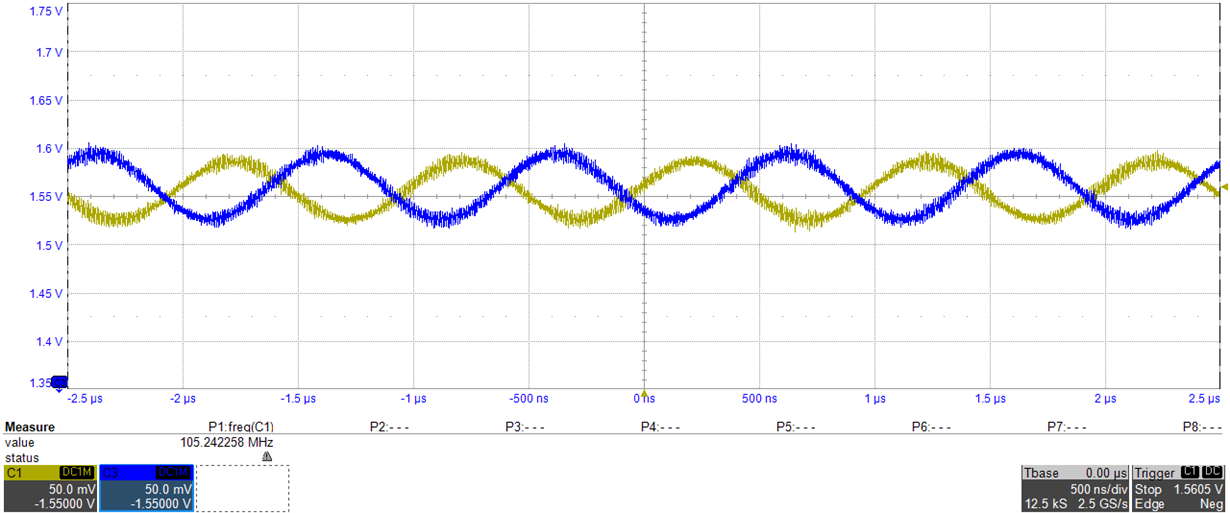
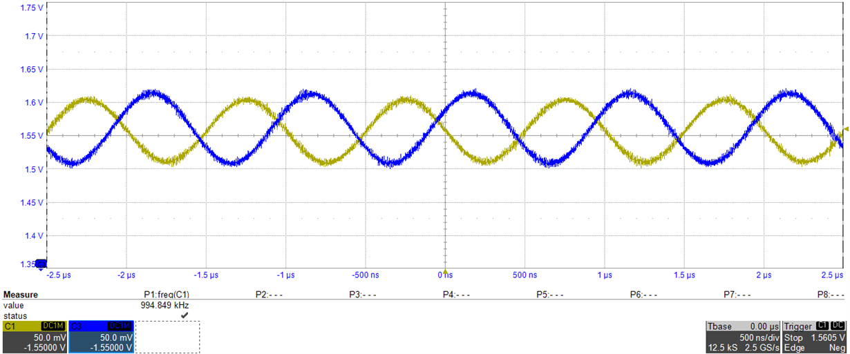
    3. I have enclosed 2 sets of waveforms showing the signals on the pins of V+ (yellow) and V- (blue). The first waveform signals give sensible conversions, the second do not. VCM is a steady 1.56V in both. There is phase and amplitude imbalance between the differential signals. Could this be the cause of the problem. Ie will the signals be rejected if the phase and/or amplitude imbalance exceeds certain values. BTW our input waveform is a single ended source and the input network to the ADC is exactly as shown in the datasheet figure 67.

  • Thanks Andrew
    I'm reviewing the latest data and the PCB layout that you provided.
    Best regards,
    Jim B
  • Andrew,

    it appears that you had a follow-on question which should be covered in a separate thread. If the problem still persists please open a new thread ideally with a spectral plot illustrating your observations.
  • I've done some further analysis based on a 100M sample rate and 1M input sine wave:

    1) An input amplitude generating approx 1/16 of the digital range consistently works.

    2) An input amplitude generating approx 1/8 of the digital range generates correct data for a few samples (<100) and then turns spurious.

    3) An input amplitude generating approx 1/4 of the digital range works correctly for approx 20 seconds before becoming spurious.

    4) An input amplitude generating approx 1/2 of the digital range works correctly for many minutes before becoming spurious.

    5) An input amplitude generating approx full digital range generates correct data for a few samples (<100) and then turns spurious.

    In all cases K28.5 (xBC) code always appears in the data immediately before it becomes spurious.

  • Hi Andrew

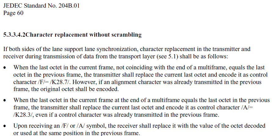
    The ADC31JB68 performs periodic alignment character insertion to be in compliance with the JESD204B spec. In your case scrambling is disabled, so the rules for Character Replacement Without Scrambling will be followed. Here is an excerpt from the standard describing the basic rules:

    Since you are not using JESD204B IP in your receive implementation this character insertion might be causing problems.

    Try setting bit 4 of Register 0x61h (JESD_CTRL2). This should disable alignment character insertion.

    Note, this register can only be changed while JESD_EN=0, so after making the change you need to re-enable the JESD204B block by setting JESD_EN=1.

    Let me know if that change has any effect on the behavior noted above.

    Best regards,

    Jim B

  • This seems to do the trick!

    I have one ADC on one board running correctly at 100M, 200M, 400M and 500M sample rates.

    When I've done some more testing, I'll close this down.

    Thanks.