This thread has been locked.

If you have a related question, please click the "Ask a related question" button in the top right corner. The newly created question will be automatically linked to this question.

ADC3424: Finding a suitable driver with SE to Diff VCM+-0.5V

Part Number: ADC3424
Other Parts Discussed in Thread: , THS4541, THS4509, LMH6554, TINA-TI

The datasheet for this ADC states that:

"Each input pin (INP, INM) must swing symmetrically between (VCM + 0.5 V) and (VCM – 0.5 V), resulting in a 2-VPP (default) differential input swing."

I honestly can't seem to find any ADC drivers with these specifications. Hopefully there would be a 3-4 channel TI IC that is compatible with this ADC. 

Thanks for any help.

  • Hello,

    I find that it is helpful to look at how the EVM's analog front end is setup.  Looking at the ADC3424EVM website, you can download the design package, and see the schematics for the analog input.

    As far as an IC that will handle these requirements, we will take a look, and get back with you soon. Our high speed amplifier group may be able to answer this question directly.

    Regards,

    Dan

  • Thanks Dan. Yeah I've been looking at those, but this is a dense PCB so I'd want a small footprint solution contained in one IC. If this is a very special ADC, perhaps I'll have to redo my design and pick another one which is more compatible with TI ADC drivers.

  • Hi Magnus,

    You could use the THS4541 ADC driver in single-ended to differential configuration for driving the ADC3424. You could take a look at the below TI Designs for the THS4541 ADC driver schematic:
    1. www.ti.com/.../TIDA-00942
    2. www.ti.com/.../TIDA-00799

    Other choices for driving the ADC3424 could be the LMH6554 and THS4509.

    Best Regards,
    Rohit
  • Great. I'm having a look at this device now. One thing though. As I understood from the ADC datasheet, the + output has a common mode voltage of VCM+0.5 and the - output - 0.5. Each individual signal swings around this common mode voltage with 1Vpp. Have I understood it correctly?
  • Yes, that is correct.

    Best Regards,
    Rohit
  • Could you please help me find that information in the ADC driver datasheet? That's my main problem now. Where are those output specifications found?

  • Hi Magnus,

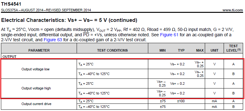
    The output specifications for the THS4541 could be found on page 6 of the datasheet which is applicable to each of the single-ended device output.

    You might want to look at the fully differential amplifier app-note for the ADC driver operation:

    Best Regards,

    Rohit

  • I'm sorry but I'm having a hard time grasping this. The equations in the App-note you linked to does not seem to me to be corresponding to the characteristics of the datasheet.

    Vout=2 Vpp <- This must basically mean Vod right?

    According to the THS4541 datasheet, Output voltage low is 0.2 V and Output voltage high is 4.8 V. What does this mean? Does it mean that Vout+ max is 4.8 V and Vout- min is 0.2 V?

    Or, does it mean that the Vout+ and Vout- are centred around respectfully 4.8 and 0.2 V?

    As you confirmed, Vout+ and Vout- ought to be centred around VCM+- 0.5V, i.e. 3.0 and 2.0 V.

    Some clarification would be highly appreciated.

  • Hi Magnus,

    Yes, the Vout = 2 Vpp means the Vod or the output differential for the ADC input or amplifier output.

    The output voltage low and high mean the Vout max is 4.8V and Vout min is 0.2V respectively, on each of the THS4541 amplifier outputs Vout+ and Vout-. This means that each THS4541 output can swing 4.6Vpp single-ended or 9.2Vpp differenetial. Since you only need 2Vpp differential, the THS4541 could easily accomplish this.

    This does not mean that the Vout + and Vout- are centered around 4.8V and 0.2V.

    The centering of the Vout+ and Vout- around VCM happens by applying a DC voltage at the Vocm input pin of the THS4541. The swing of +/-0.5V (or higher if needed) at the THS4541 Vout+ and Vout- then happens centered around this Vocm voltage. It is usually required that this Vocm voltage at the amplifier be equal to the VCM voltage at the ADC. You might want to take a look at Figure 76 in the THS4541 datasheet for the VOCM interface between the amplifier and the ADC.

    Best Regards,
    Rohit
  • Thanks. I suppose it was the +-05V offset that confused me since I haven't been able to find that anywhere. How do I control this? I suppose gain by definition is the voltage swing on each output and it doesn't have anything to do with their offset.

  • Magnus,

    What +/-0.5V offset are you referring to for the THS4541?

    Best Regards,
    Rohit
  • Vout+ will swing around Vocm+0.5V and Vout- will swing around -0.5V right? You mentioned that this offset could be larger?

  • To answer your question more thoroughly:

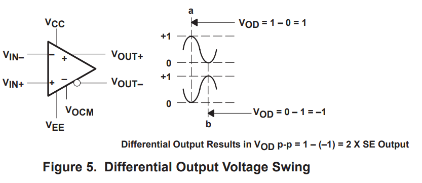
    We have established now that Vocm is the average of the two outputs, Vout+ and Vout-. Vout = 2Vpp in the Electrical Characteristics of the THS4541 datasheet.I suppose that is the total difference, which in the figure below is 2V+ the offset I'm talking about. At Vin=0, Vout+ and Vout- will not be the same, because of this offset. This is the Vcm+-0.5V we've been talking about, right?
    Gain by itself is the increase in swing on each output. I want to know how to control this +-0.5V offset (The centre of Vout+ - Vout- in the figure below).

  • Magnus,

    The average value of the THS4541 output swing is controlled by the Vocm pin voltage. For example, if the Vocm pin voltage is 1V, then the {(Vout+)+(Vout-)}/2 will be 1V. Any output swing of the THS4541 will occur centered around this Vocm voltage. The THS4541 has rail-to-rail output stage, so you have plenty of output swing headroom in-order to swing close to 2Vppd at the ADC input.

    You could simulate your ADC driver circuit in TINA-TI and attached is the same. THS4541_ADCDriver.TSC

    Best Regards,

    Rohit

  • I see it now. It was confusing me, the figure where the two output signals seem to have an offset. Now I see that they don't and that's just a way to explain the effective 2Vpp.
    This sentence from the ADC datasheet confused me:

    "Each input pin (INP, INM) must swing symmetrically between (VCM + 0.5 V) and (VCM – 0.5 V), resulting in a 2-VPP (default) differential input swing."


    So the ADC datasheet talks about 2-VPP as effective, while the actual voltage swing is 1V. The ADC driver is using actual voltage swing as the VPP definition, meaning that 1Vinput will correspond to both outputs swinging between VCM-0.5 to VCM+0.5.