• Join
  • Sign In with my.TI Login
Texas Instruments
  • Products
  • Applications
  • Tools & Software
  • Support & Community
  • Sample & Buy
  • About TI
Sample & Purchase Cart Sample & Purchase Cart
  • Search
  • Advanced
TI E2E™ Community
  • Support Forums
  • Blogs
  • Groups
  • Videos
  • 简体中文
  • More ...
TI Home » TI E2E Community » Support Forums » Data Converters » Precision Data Converters » Precision Data Converters Forum » DAC7821
Share
Precision Data Converters
  • Forum
  • Files
  • E2E Wiki
Options
  • Subscribe via RSS
Check out
The Signal blog
  • $core_v2_blog.Current.Name

    Grounding Principles

    Posted 4 days ago
    by Bruce Trump
    In a previous blog on supply bypassing , I cautioned that poor...
  • $core_v2_blog.Current.Name

    Handy Gadgets and Resistor Divider Calculations

    Posted 11 days ago
    by Bruce Trump
    Handy gadgets make our engineering life easier—the little...
  • $core_v2_blog.Current.Name

    Chopper Op Amps—are they really noisy?

    Posted 19 days ago
    by Bruce Trump
    Chopper op amps offer very low offset voltage and dramatically...

DAC7821

DAC7821

This question is answered
eli
Posted by eli
on Apr 05 2012 00:28 AM
Genius3640 points

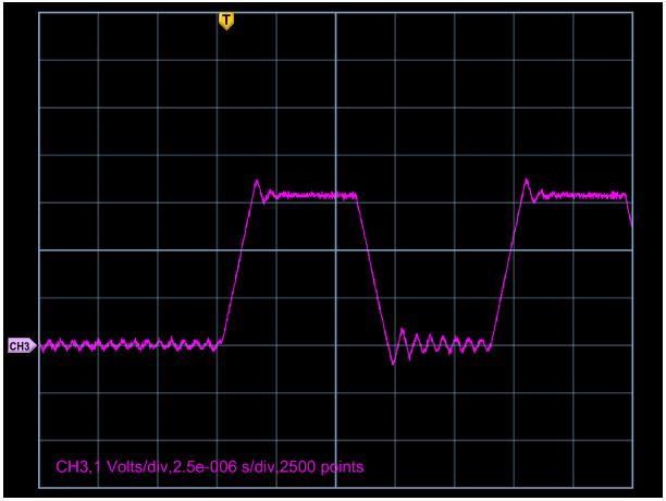
 we apply a pulse train of zeros and ones .

 5287.dac7821_ CHANNEL23.pdfThe output should be 0v to 3.3v 
 
Can you tell me what is the settling time from strobe at TP10 to output at TP7
 
According to the datasheets ?.
 
Is there a way to improve the response time ?.
 
dac7821
Report Abuse
  • Reply
You have posted to a forum that requires a moderator to approve posts before they are publicly available.
All Replies
  • Tom Hendrick
    Posted by Tom Hendrick
    on Apr 06 2012 09:18 AM
    Verified Answer
    Verified by Tom Hendrick
    Guru86220 points

    Hi Eli,

    Take a look at Figure 11 on page 7 of the DAC7821 data sheet.  The output transition should take about 50ns.  In Table 1 starting on page 12 of the DAC7821 data sheet, you will find some details on various amplifiers you can use with this MDAC.  Take a look over the choices listed and see what fits your power budget.

    The OPA277 you are using currently has a slew rate of only .8V/us which is going to be the limiting factor on your settling time at TP7.  Changing to the OPA727 would give you a slew rate of 30V/us - significantly faster but that comes at the cost of higher power consumption. 


    Regards,

    Tom

    Report Abuse
    • Reply
    You have posted to a forum that requires a moderator to approve posts before they are publicly available.
  • eli
    Posted by eli
    on May 07 2012 14:43 PM
    Genius3640 points
    Attached 3 files.
     
    Attached 3 files
    2084.dac_v1.pdf
    1.     DAC board that uses the TI chip DAC7821.
     
    2.    Small output signal
           
           The  data of one of the DAC7821 is set to 400 and to 0 and vice versa .
     
    3.     Large output signal
           
           The  data of one of the DAC7821 is set to 4096 and to 0 and vice versa .
     
     
    Can you explain the ringing , What should I do to avoid them.
    dac7821
    Report Abuse
    • Reply
    You have posted to a forum that requires a moderator to approve posts before they are publicly available.
  • Tony Calabria
    Posted by Tony Calabria
    on May 09 2012 14:26 PM
    Mastermind42750 points

    Hi Eli,

    The file that you attached is the schematic. Is there another picture that you wanted to attach that shows the three files and pictures of the performance that you see?

    A couple comments on the DAC and your schematic-

    - You will want to avoid using the same source for the reference and the power supply. Any ripple on the power supply will couple through the reference and out the output of the DAC. Additionally, MDAC's generally prefer a buffered reference voltage to help source the current to the device.

    - You will want a 1-10uF capacitor on the reference pin of the DAC to help clean and stabilize the reference voltage.

    - Take a look at the DAC glitch spec to get an idea of what behavior to expect during a DAC output update. Figure 9 we show what the glitch would look like a midscale (worst case) but you should expect to see some glitch behavior at all DAC updates. If you can send pictures showing the ringing behavior, I can compare to see if it is comparable to what we would expect.

    Regards,

    Tony Calabria

    Report Abuse
    • Reply
    You have posted to a forum that requires a moderator to approve posts before they are publicly available.
  • eli
    Posted by eli
    on May 09 2012 23:54 PM
    Genius3640 points

    Above are two picture.

    Please advise

    B.regards

    Eli

    dac7821
    Report Abuse
    • Reply
    You have posted to a forum that requires a moderator to approve posts before they are publicly available.
  • Tony Calabria
    Posted by Tony Calabria
    on May 10 2012 16:55 PM
    Mastermind42750 points

    Hi Eli,

    Top picture looks like you may have some grounding issues. The bottom picture points more to switch charge injection from the internal R2R DAC. You will want to add a 1-10uF capacitor on the Vref line as well as a small capacitor on TP1 and TP2 to help clean up the signal.

    Regards,

    Tony Calabria

    Report Abuse
    • Reply
    You have posted to a forum that requires a moderator to approve posts before they are publicly available.
TI E2E™ Community
  • Support Forums
  • Blogs
  • Videos
  • Groups
  • Site Support & Feedback
  • Settings
TI E2E™ Community Groups
  • TI University Program
  • Make the Switch
  • Microcontroller Projects
  • Motor Drive & Control
Other Communities
  • Deyisupport
  • Designsomething.org
  • beagleboard.org
  • TI on Element 14
  • TI on TechXchangeSM
Other Technical & Support Resources
  • WEBENCH® Design Center
  • Product Information Centers
  • Technical Documents
  • TI Design Network
  • TI Technical Articles
  • TI Training

All content and materials on this site are provided "as is". TI and its respective suppliers and providers of content make no representations about the suitability of these materials for any purpose and disclaim all warranties and conditions with regard to these materials, including but not limited to all implied warranties and conditions of merchantability, fitness for a particular purpose, title and non-infringement of any third party intellectual property right. TI and its respective suppliers and providers of content make no representations about the suitability of these materials for any purpose and disclaim all warranties and conditions with respect to these materials. No license, either express or implied, by estoppel or otherwise, is granted by TI. Use of the information on this site may require a license from a third party, or a license from TI.

Content on this site may contain or be subject to specific guidelines or limitations on use. All postings and use of the content on this site are subject to the Terms of Use of the site; third parties using this content agree to abide by any limitations or guidelines and to comply with the Terms of Use of this site. TI, its suppliers and providers of content reserve the right to make corrections, deletions, modifications, enhancements, improvements and other changes to the content and materials, its products, programs and services at any time or to move or discontinue any content, products, programs, or services without notice.

Follow Us Texas Instruments on Facebook Texas Instruments on Twitter Texas Instruments on LinkedIn Texas Instruments on Google+
TI Worldwide | Contact Us | my.TI Login | Site Map | Corporate Citizenship | mobile m.ti.com (Mobile Version)

TI is a global semiconductor design and manufacturing company. Innovate with 100,000+ analog ICs and
embedded processors, along with software, tools and the industry’s largest sales/support staff.

© Copyright 1995-2013 Texas Instruments Incorporated. All rights reserved.
Trademarks | Privacy Policy | Terms of Use