This thread has been locked.

If you have a related question, please click the "Ask a related question" button in the top right corner. The newly created question will be automatically linked to this question.

ADS8556 - No signal on SDO_A

Other Parts Discussed in Thread: ADS8556

Hi,

I would like to use an ADS8556 in software mode and serial interface (with a SPI).

I am using ADS8556EVM. So here is the jumpers configuration:
- JP1,JP2,JP5,JP6,JP7,JP8 : 1.2
- JP3 : 7.8
- JP4, JP10, JP11 : 2.3
- JP9 : 1.2, 4.5, 7.8
- JP12 : close

The switch SW1 configuration is :
- word
- 4x
- SFT
- SER
- REFBUF ENA : 1
- Daisy chain ena : 0
- SERA enable : 1
- SERB enable : 0
- SERC enable : 0
- REFen : 1

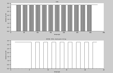
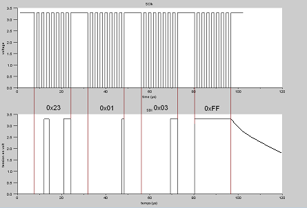
The value of the control register is : 0xE30103FF (sent to SDI pin)

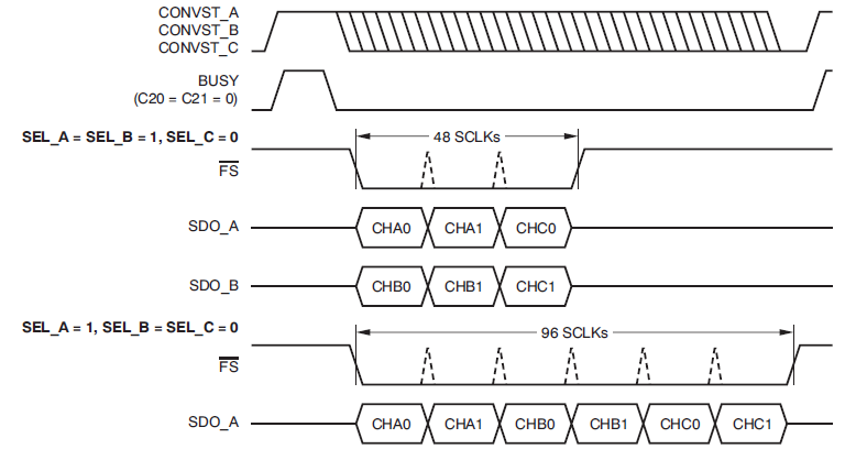
Even if I am working in serial mode, I have to use DC_TOUT and DC_INTa pins on the parallel control port (for CONVST_A and BUSY respectively). Am I wrong ?

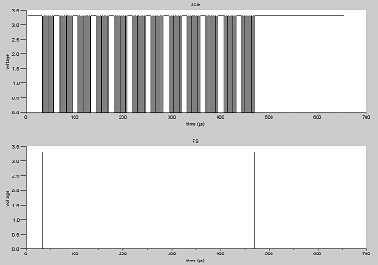
Unfortunately, I have no signal on SDO_A ouput ( I only use this pin to read the converted data of all analog inputs).

Thanks in advance for any idea to solve my problem.

Regards

  • Hi Maelenn,

    Your switch and configuration register settings for the ADS8556 sound correct.  What is the status of the STBY pin?  You can check this on U3 pin 7.  In the ADS8556EVM default configuration, the pull ups on the A, B, C inputs to U3 should drive Y7 low which would put the ADS8556 into stand-by mode.  Putting a shunt jumper on J4 pins 7-8 should take care of that.  CONVST and BUSY are wired to J4 only, but you could short them across to any unused pins on J1 if you like.  The CONVST could also be applied directly to JP9.

  • Hi Tom,

    Thank you for your answer.

    The status of the /STBY pin is high, so the converter is not in standby mode. I put a shunt jumper on J4 pins 7-8 but I have still not received any bit.


    Maybe it is a software problem.
    Here are the steps of my program:

    - Initialization of UART
    - Initialization of SPI
    - Initialization of CONVST_A and BUSY

    ___in an infinite loop_______________
    - CONVST_A = 1
    - Wait for busy status low
    - Enable /FS
    - Transfer of 12 bytes (400000 bps)
    - Disable /FS
    - Disable CONVST_A
    - Wait for 1second
    ------------------------------

    Thanks in advance for any answer.

    Regards,

    Maelenn

  • Hi Maelenn,

    Can you grab a screen shot of SCLK and SDI along with FS/CS during your initialization cycle?

  • Hi Tom,

    I am sorry, I am not able to give you any screenshots because my scope has no computer connection and I cannot take good photos of it.

    Have you got typical screenshots of what you asked for? Could you post them or send them to me? In this way, I will compare your results to mine.

    Thanks in advance,

    Maelenn

  • Hi Maelenn,

    My apologies for the delay here - I've been traveling and have not had time to try and capture these waveforms for you.  What is your current status?  Have you made any headway on getting the data from SDOA of the ADS8556?

  • Hi Tom,

    I am always trying to have conversion results on SDO_A. As I cannot show any scope screenshot, I have approximatively reproduced the signals on SCILAB.

    The first picture shows the SCLK

    The second picture shows SCLK and SDI (only the first 2 bytes). At the end of CR (SDI) the signal is decreasing slowly until 0V.

    The third picture shows the SCLK and the FS signal.

    Regards,

    Maelenn

  • It is better with the third one :

  • Maelenn,

    The /RD pin also needs to be pulled low for using the serial interface in software mode. You can just apply a shunt from J4.5-J4.6. Also, ensure that JP3.7-JP3.8 is applied correctly. The orientation on the physical board versus the schematic in the UG is a little deceptive but the board has JP3.7 labeled in silkscreen.

    Let us know your results.

  • Hi,

    I apply a shunt from J4.5-J4.6. But I have got no more results. Do I have to put another one from J4.3-J4.4 too?

    When I check the signal of JP3.7-8 shunt, it is always high is it normal?

    I've got two more questions:

    - Do I have to connect external serial clock on J6 in serial interface software mode? Because the datasheet of ADS8556 doesn't mention (if I am not mistaken) that external clock is compulsory while the datasheet of ADS8556EMV does: "When using software mode, the user must apply an external conversion clock to SMA connector J6."

    - I connected AGND and DGND together. Is it correct?

    Thanks in advance for your answers.

    Regards,

  • Maelenn,

    Maelenn Cabon said:
    I apply a shunt from J4.5-J4.6. But I have got no more results. Do I have to put another one from J4.3-J4.4 too?

    It shouldn't be necessary, but wouldn't hurt.

    Maelenn Cabon said:
    When I check the signal of JP3.7-8 shunt, it is always high is it normal?

    JP3.7-8 routes the /CS signal from J1.7/J1.9 to the ADS8556. This signal should not stay high, it should be controlled by your micro-controller's serial interface peripheral and behave as described in the ADS8556 datasheet, see below:

    Maelenn Cabon said:
    - Do I have to connect external serial clock on J6 in serial interface software mode? Because the datasheet of ADS8556 doesn't mention (if I am not mistaken) that external clock is compulsory while the datasheet of ADS8556EMV does: "When using software mode, the user must apply an external conversion clock to SMA connector J6.

    The necessity of an external conversion clock should remain dependent on the configuration register settings. It is not always required in software mode.

    Maelenn Cabon said:
    - I connected AGND and DGND together. Is it correct?

    Yes.

    Investigate your CS issue. If your micro cannot sink the current to pull the pin low consider removing the pull up resistor.

  • Hi Kevin,

    I receive some data now!

    But I only receive data from channel C (CH_C0 and CH_C1).

    I tried further values for the control register but I only got the converted data of channels C0 and C1.
    For the others, I receive 0x7FFE (whatever the input signal on channels A0 - A1 - B0 - B1).
    (For example I sent CR = 0x42 01 63 FF to receive CH_B0 and 1, without success, I still receive only the data of channels CH_C0 and 1)

    I tried to see the control register value in output too. But I did not succeed. (I sent 0x 02 03 E3 FF)

    Could you please tell me the value of the control register to receive all data (I tried 0x E2 01 03 FF) and to see the control register?

    Thanks in advance,

    Maelenn

  • Maelenn,

    Glad we've made some progress. I have a few more notes for you. Lets start by looking at the values you've mentioned writing to the configuration register & their outcomes.

    Maelenn Cabon said:
    I tried further values for the control register but I only got the converted data of channels C0 and C1.
    For the others, I receive 0x7FFE (whatever the input signal on channels A0 - A1 - B0 - B1).
    (For example I sent CR = 0x42 01 63 FF to receive CH_B0 and 1, without success, I still receive only the data of channels CH_C0 and 1)

    Hex Word: 0x420163FF

    Bit Grouping: 000-000-0-0-0-0-00-0-0-0-0-000-0-00-0000000000
    Word Value: 010-000-1-0-0-0-00-0-0-0-1-011-0-00-1111111111

    Device Configuration:
    Channel Pair B Enabled, A & C disabled for next conversion
    Input Range 4Vref on A, B, C
    Internal Reference Enabled
    Internal Reference Buffer Disabled
    2.5V Reference
    Channel Pair C Normal Operation, A & B Power-Down
    REFDAC Fullscale

    Under this configuration you have channel pairs A & C disabled for the next conversion and channel pairs A & B in power-down mode. This is not a valid configuration register configuration, so your results may be very unexpected as you have described here.

    Maelenn Cabon said:
    I tried to see the control register value in output too. But I did not succeed. (I sent 0x 02 03 E3 FF)

    Hex Word: 0x0203E3FF
    Bit Grouping: 000-000-0-0-0-0-00-0-0-0-0-000-0-00-0000000000
    Word Value: 000-000-1-0-0-0-00-0-0-1-1-111-0-00-1111111111

    Device Configuration:
    Channel Pairs A, B, C Disabled for next conversion
    Input Range 4Vref on A, B, C
    Internal Reference Enabled
    Internal Reference Buffer Disabled
    2.5V Reference
    Output CR on SDO
    Channel Pairs A, B, C Power Down
    REFDAC Fullscale

    These settings look correct. You mention that you 'did not succeed', what did happen?

    Maelenn Cabon said:
    Could you please tell me the value of the control register to receive all data (I tried 0x E2 01 03 FF) and to see the control register?

    Hex Word: 0xE20103FF
    Bit Grouping: 000-000-0-0-0-0-00-0-0-0-0-000-0-00-0000000000
    Word Value: 111-000-1-0-0-0-00-0-0-0-1-000-0-00-1111111111

    Device Configuration:
    Channel Pairs A, B, C Enabled for next conversion
    Input Range 4Vref on A, B, C
    Internal Reference Enabled
    Internal Reference Buffer Disabled
    2.5 Reference
    Channel Pairs A, B, C normal operation
    REFDAC Fullscale

    This configuration should be correct to convert channel pairs A, B, and C on the next conversion cycle assuming your CONVST signals are behaving appropriately. When you tried this configuration what results did you see?


    In all of the configuration register permutations above, the internal reference buffers are disabled. We haven't really looked at your analog configuration with the device yet, but since you have the internal reference enabled I expect that you're attempting to use it. In the figure below all of the buffers highlighted in red are disabled if you do not enable the internal reference buffers:

    For any additional information about the internal reference and it's buffers, please consult the product datasheet. Specifically, page 25.

    With the internal reference buffers disabled I would expect that many of your conversion results are going to rail out and give codes that are full-scale. Try enabling the buffers and let us know your results. 

  • Hi Kevin,

    When I put the same signal on CH_XX inputs (which is a sine wave [-2;2]V) , in software mode (SW1_3.18 left on the emv), whatever the CR I send
    (0xE2(or3)0103FF, 0x22(or3)01C3FF, 0x42(or3)01A3FF, 0x82(or3)0163FF, 0x02(or3)03E3FF)
    - I receive the same value for ch-ao cha1 ch-bo ch-b1 which is continuous (it is the last value recorded in buffers I think)
    - But I receive the good value of the sine wave on ch-c0 ch-c1 

    It seems like the ADS8556 do not read the CR 

    But when I put SW1_3.18 right (hardware mode), I have got the correct value of all the inputs (whatever the CR I have sent before)

    According to the datasheet of ADS8556 page 29, the internal reference source is disabled by default but the internal reference buffer is enabled by default, that's why I put this bit at 0. But as you recommended, I put this bit at 1 but I receive the same values as before.

  • Maelenn,

    You are correct, I forgot about the inversion of the buffer enable bits. I'll be checking into this some more tomorrow.

  • Maelenn,

    Sorry for the delayed response here, I had some personal issues to attend to over the last few days that kept me from office. We've replicated your test setup and results and will be working on finding the solution. Unfortunately many of us will be traveling next week and will be bandwidth limited, so it may be a bit until we are able to sit down with this.

  • OK, no problem.

    I will let you know if I get ride of this control register problem.

    Thanks,

  • Maelenn,

    I apologize for the delay getting back to you, I hope to be able to revisit this soon. Any updates?