This thread has been locked.

If you have a related question, please click the "Ask a related question" button in the top right corner. The newly created question will be automatically linked to this question.

ADS1299 Wiring & Start

Other Parts Discussed in Thread: ADS1299

Hello,

I'm trying to get the ADS1299 running. I wired the chip after the Instructions in the Quick Start Guide, programmed parts of the Startup Sequence.
For testing the functionality, instead of starting the internal signal generator, I just tried to read the ID from the first register. I don't get the response I expected so I'm wondering, if I got the wiring and the startup Sequence right. My Oscilloscope is broken so i dont have any Information about the Transfered Data. English is not my native languange (please excuse the lack of correct grammar & spelling) and I'm still studying (this is a preparation for my bachelor thesis), therefore i would like to know if i got the instructions right. I tried to find errors but the wiring seems right & the code just leaves me one Question (The SPI clock).

My wiring:

5V --> pins 56,59,21,22,19
3,3V -> pin 48
GND -> pins 49, 23, 25, 32, 31
with condensator to ground : 24, 26 ,28, 30,  55 and the pins above

SPI:
MOSI    -> pin 34
MISO    -> pin 43
!CS       -> pin 39
SLCK   -> pin 40

Startup:
!PWDN   -> pin 35
!RESET  -> pin 36
START    -> pin 38
CLKSEL -> pin 52

and here my (shortend) Startup Sequence with the attempt to read the ID in Python

#SPI Device init
spi = spidev.SpiDev()
spi.open(0,0)
spi.max_speed_hz = 100000 # I'm not sure about the frecuency here

#GPIO PINS:
pwdn = 23 cs = 24 reset = 25 start = 18 clksel = 17 #GPIO init GPIO.setmode(GPIO.BCM) GPIO.setup(pwdn, GPIO.OUT) GPIO.setup(cs, GPIO.OUT) GPIO.setup(reset, GPIO.OUT) GPIO.setup(start, GPIO.OUT) GPIO.setup(clksel, GPIO.OUT)
#Startup:
#All Signals LOW GPIO.output(pwdn, False) GPIO.output(clksel, False) GPIO.output(cs, False) GPIO.output(reset, False) GPIO.output(start, False)
sleep
(1)
#!CLKSEL HIGH
GPIO.output(clksel, True) sleep(1)

 #!PWDN HIGH, !RESET = HIGH

GPIO.output(pwdn, True) GPIO.output(reset, True) sleep(1)

 #!RESET LOW GPIO.output(reset, False) sleep(0.5)

 #!RESET HIGH GPIO.output(reset, True) sleep(1)

 #SEND SDATAC data1=spi.xfer2([17]) #xfer sends an array of Bytes and stores the Answer in the specified Variable sleep(1)

 #SEND WREG CONFIG4 E0h data2=spi.xfer2([67,0,104]) sleep(1)

 #READ REGISTER 00

 # Bits to Send: 0010 0000 0000 0000 -> 32, 0 data3 = spi.xfer2([32,0])

I'm using a Python Wrapper for the SPI Communication. This worked with other Chips. Besides the SPI clock I cant find anything ....

It would be really nice if you could comment on wether my Setup or startup contains any basic errors.
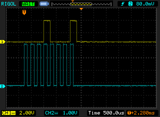
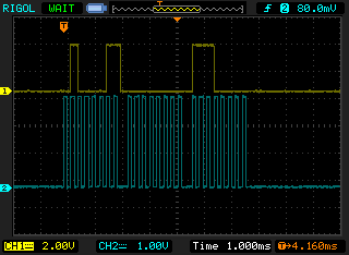
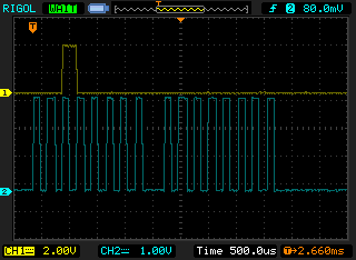
I'try to get another Oscilloscope to record the SPI Signal, but this could last a week or more...

Thank you very much!!

Till

  • Hi Till,

    Apologies for the delay in getting back to you!  Have you made any headway here?  Is is possible for you to send along a screen shot (O-Scope or Logic Analyzer) of the communication interface to us?  The code sequence above seems OK, but it's often easier for us to just review the actual SPI data transmitted from your host without having to dig through the peripheral details.

  • Hi Tom,

    no Problem! Since my Scope is still broke and i won't have it back until two or more weeks, i didn't make any progress here. I'll post the images once my osci arrived. Thanks & Greetings

    Till

  • Hey, 

    now i have another scope. Since i only have two channels, what would be interesting to see? 

    Until now i couldn't get any Answer from the chip.

    Greetings

    Till

    EDIT:

    Here is a picture of the SPI Clock (blue) and the SDATAC Command.


  • Hello,

    i´m still unable to get any response from the chip. Is there anyway to check if the chip is working?

    Would it be possible to samlpe another chip if this one doesnt work?

    Greetings

  • Any Idea? I'm still stuck with this chip. I'm can see my device sending the commands but there is just no answer from the chip. I'm pretty sure about the wiring & just want to know if the execution of the code above should give me an answer from the device or if there is somethin wrong with the routine. What oscilloscope image would help you? 

    Greetings 

    Till

  • Ok,

    some more Details.

    Im Using a Raspberry Pi to connect to the ADS1299. Basicly its the bcm2835. Because i didnt want to write my own spi kernel Driver i used the spi-dev together with this very simple library: http://www.airspayce.com/mikem/bcm2835/index.html 

    I rewrote the Code in C to make it more understandable. I also double checked the whole wiring. Nevertheless i`m not able to read a register.

    I would be very glad about any suggestions.

    Greetings

    Till Sellschopp

    //----------------------------------------------------------------

    #include <bcm2835.h> //Library for the bcm2835
    #include <stdio.h>
    #include <stdlib.h>

    //define GPIO PIN Numbers

    #define RESET RPI_GPIO_P1_11
    #define PWDN RPI_GPIO_P1_12
    #define START RPI_GPIO_P1_15
    #define DRDY RPI_GPIO_P1_16
    #define CLKSEL RPI_GPIO_P1_18
    #define SDATAC 0x11

    //------------------------------------------------


    int main(int argc, char **argv){


              //load library

             if((bcm2835_init())<0){
                    printf("Could not load the bcm2835 library \n");
                    exit(1);
             }
             printf("Library loaded \n");

             //Set GPIO Pins to Output

             bcm2835_gpio_fsel(RESET,BCM2835_GPIO_FSEL_OUTP);
             bcm2835_gpio_fsel(PWDN,BCM2835_GPIO_FSEL_OUTP);
             bcm2835_gpio_fsel(START,BCM2835_GPIO_FSEL_OUTP);
             bcm2835_gpio_fsel(DRDY,BCM2835_GPIO_FSEL_OUTP);
             bcm2835_gpio_fsel(CLKSEL,BCM2835_GPIO_FSEL_OUTP);

             //initiate SPI
             bcm2835_spi_begin();
             bcm2835_spi_setBitOrder(BCM2835_SPI_BIT_ORDER_MSBFIRST);
             bcm2835_spi_setDataMode(BCM2835_SPI_MODE1);
             bcm2835_spi_setClockDivider(BCM2835_SPI_CLOCK_DIVIDER_65536);
             bcm2835_spi_chipSelect(BCM2835_SPI_CS0);
             bcm2835_spi_setChipSelectPolarity(BCM2835_SPI_CS0, LOW);


             // POWERUP Sequenz S.58, FIG 56
             // ALL INPUTS LOW
             bcm2835_gpio_write(RESET,LOW);
             bcm2835_gpio_write(PWDN,LOW);
             bcm2835_gpio_write(START,LOW);
             bcm2835_gpio_write(DRDY,LOW);

             bcm2835_gpio_write(CLKSEL,LOW);
             // CLKSEL -> 1 , wait
             bcm2835_gpio_write(CLKSEL,HIGH);
             bcm2835_delay(500);
             // PDWN -> 1, RESET -> 1, wait 1s
             bcm2835_gpio_write(PWDN, HIGH);
             bcm2835_gpio_write(RESET,HIGH);
             bcm2835_delay(1000);
             // RESET PULSE
             bcm2835_gpio_write(RESET,LOW);
             bcm2835_delay(50);
             bcm2835_gpio_write(RESET,HIGH);

             printf("Power-Up Done \n");
             bcm2835_delay(50);
             // send SDATAC
             int error;
             error = bcm2835_spi_transfer(SDATAC);

             printf("SDATAC sent \n");

             //set Internal Reference
             char write[] = { 0x43 , 0x00 , 0xE0 };
             bcm2835_spi_transfern(write, sizeof(write));

             printf("Internal Reference set \n");

             //Read Register
             char read[] = { 0x20 , 0x00 };
             bcm2835_spi_transfern(read, sizeof(read));
             printf("Data Read: %X , %X \n", read[0], read[1]);
             //Close Device
             bcm2835_spi_end();
             bcm2835_close();
             printf("bye bye \n");
             return 0;
    }

  • Good Day again. I'm not sure if my Question is stupid or to much to ask for, but i would apreciate a comment on this topic. Here are some Scope images..

    SDATAC

    Set internal Reference:

    Read Register:

    and nothing on the MISO....

  • anyone, anything? ....

  • Hi 

    Have a look at the other signals on the SPI interface there is SPI_in and SPI_out (which have you shown on the graphs?) What is the START signal and the CE signals doing??

  • Hi,

    the Graphs show the MOSI (Data in of the Chip) and the Clock. There is no signal on the Data out (MOSI) line. For testing i have the Chip Select permanently at GND and the START Pin is LOW during the Transmission.

    Thanks & Greetings

    Till

  • Hi,

    This may be late for you, but looking at the read command, you should wait for another byte to get the answer back, that is issue another 8 clock cycles. Because what you do is just send the command there (two bytes), but you also need to have the clock active to read the register value. Just send an 8-byte zero value after the register read command.


  • Hey Cosmin,

    thanks a lot! This solved everything & its working now :-)

    Greetings

  • Hi Till,

    I wanted to do same, do you have final code somewhere shared?

    It will be very helpful for me.

    Thanks,

    Ali

  • Hey,

    i do this for my thesis and my university does not allow me to publish anything before I finish the work. Afterwards I will share the Thesis and the whole code on a git repo. The code I posted above (in C) is basically working. I can try to help you if you have questions.

    Greetings

  • Hello Chuchaki,

    is your thesis finished well?

    Can you now post your Code.

    May hep to solve problems.

    Regards

  • Hi Chuchaki

    I'm very interested in your thesis as well, please let me know if you publish the results. 

    I have 2 questions. 1. Once you run the power-up sequence, could I program the ADS1299 normally with spi? Is entirely necessary the power-up sequence? and 2. How can I visualize the output of the signal as you show in the scope? Is it through SPI out or how is it? 

    Thanks, regards.

    Felipe

  • Hey Felipe,

    excuse for the huge delay. I was backpacking through Latin-America for some time. If  there still is interest in code and thesis, i can create a git repository and do kind of an HowTo. Would take a little, but i would do that. The Thesis is written in German and currently i wont have the time to translate it. But i can upload it too. 

    About your questions: 
    1) The Power Up Sequenze is entirely necessary to guarantee a porper boot of the device.  And after the boot you can read and write the register as well as start and read measurement via SPI.
    2) To Display the Communication I used a logic analyser from Saleae. Great little device by the way ;-)

    Let me know if someone is interested in a git repo. 

    regards,


    Till

  • Hello Till,

    a posibility to read your theses would be nice. Also a How To is great idea.

    I am still interested and seeking up every information about ADS129x I can get.

    regards,

    Melanie


  • Hi Meanie,

    These people are working on ADS1299 and Arduino and have some code here. You may need to tweak it for Raspberry PI

    https://github.com/OpenBCI

    And also here.

    https://github.com/conorrussomanno/ADS1299 

    Thanks,
    Ali

  • Hey Till,

    Can you please upload the final code for the startup sequence for ADS1299 and wiring information?

    Regards

    Qamar