This thread has been locked.

If you have a related question, please click the "Ask a related question" button in the top right corner. The newly created question will be automatically linked to this question.

ADS1299 Issue -- Can't modify CH5SET, CH6SET, CH7SET, and CH8SET Registers

Other Parts Discussed in Thread: ADS1299, ADS1298

Hi All,

This is the second time I've run across this, so I'm hoping that someone else has seen it as well.  I am configuring an ADS1299 by writing data to the registers.  As a verification, I read the data back.  Invariably, CH5SET..CH8SET all read back as 0x61, although I'm trying to write them as 0x00.

Any ideas as to what would cause this?

I'm reasonably certain it is not an issue with the code that is updating the registers -- I can modify and read back CH1SET..CH4SET, and there is an ADS1298 attached to my system that I can modify without issue (and I've verified it on both a Logic Analyzer and a scope)

I'm not sure if it is important, but the ID register is 0x20, which is odd, since I think it should be 0x1e.

Any help would be appreciated,

Brian LeLacheur

Natus

  • Hi Brian,

    Let's focus on debugging the ID register first. You are correct, it is supposed to be 0x1E. This register is Factory-Programmed, Read-Only. What command are you writing to read-back the ID register? Have you verified this command with an oscilloscope vs the Logic Analyzer? With an oscilloscope, you can see if you have noise on the clocking and data lines.


    Is this problem repeatable? Or does the ID register only read back 0x20 at times, and 0x1E at other times?


    Thanks,


  • Hi Ryan,

    Okay, ID Register it is.  The command that I use to read the ID register is:  0x20 0x18 followed by 15 0x00.  This is my general read register command.  I have verified it with both a scope and a protocol analyzer.  On the scope, all the signals look good -- The SPI data lines are good, and the CLK looks good.

    Note, after we power up the board, we send an SDATAC command, then write our desired configuration to the registers.  This configuration overwrites registers 1 through 24 with our desired values.  The CH?SET registers are set to 0x00 in this situation.  So, the normal process we follow is:

    SDATAC

    WREG 1, 23 registers with data: 0xD6, 0xC0, 0xE0, 0x00, 0x00, 0x00, 0x00, 0x00, 0x00, 0x00, 0x00, 0x00, 0x00, 0x00, 0x00, 0x00, 0x00, 0x00, 0x00, 0x0F, 0x00, 0x00, 0x00

    Our Read command is:

    RREG 0, 25 registers

    The problem is very repeatable.  When a chip is acting like this (and it seems that a very high percentage of them are), it tends to always read this way.  We have never seen a situation where the ID register was corrupted, then on the next read a different register was corrupted.  When this happens, it tends to alway be that the id register reads as 0x20, and registers 9, A, B, and C are the default value of 0x61.  We occasionally see that registers 9..C are set to 61610000, with registers B and C also being unmodifiable.

    Does this lead you anywhere?

    Thanks!

    Brian

  • Hi Brian,


    Thanks for the information. I'm going to talk with the chip designer tomorrow and get back to you afterwards. He may have a better idea of what is causing this problem.


    Regards,

  • Hi Brian,


    This may be an OTP issue, since it is coming up as a 4-channel device. Can you issue a RESET and tell us what the register reads back?


    Thanks,

  • Hi Ryan,

    Okay, here it goes:  After we ready the chip, I issued the following commands:

    1. SDATAC (0x11)
    2. RREG 0, 24 (0x20, 0x15) which gives 0x20, 0x96, 0xc0, 0x60, 0x00, 0x61, 0x61, 0x61, 0x61, 0x00, 0x00, 0x00, 0x00, 0x00, 0x00, 0x00, 0x00, 0x00, 0x00, 0x00, 0x0f, 0x00, 0x00, 0x00
    3. WREG 1, 23 (0x41, 0x14) writing 0xD6, 0xC0, 0xE0, 0x00, 0x00, 0x00, 0x00, 0x00, 0x00, 0x00, 0x00, 0x00, 0x00, 0x00, 0x00, 0x00, 0x00, 0x00, 0x00, 0x0F, 0x00, 0x00, 0x00
    4. RREG 0, 24 (0x20, 0x15) which gives 0x20, 0xd6, 0xc0, 0xe0, 0x00, 0x00, 0x00, 0x00, 0x00, 0x00, 0x00, 0x00, 0x00, 0x00, 0x00, 0x00, 0x00, 0x00, 0x00, 0x00, 0x0f, 0x00, 0x00, 0x00
    5. RESET (0x06)
    6. delay 20ms
    7. SDATAC (0x11)
    8. RREG 0, 24 (0x20, 0x15) which gives 0x20, 0x96, 0xc0, 0x60, 0x00, 0x61, 0x61, 0x61, 0x61, 0x00, 0x00, 0x00, 0x00, 0x00, 0x00, 0x00, 0x00, 0x00, 0x00, 0x00, 0x0f, 0x00, 0x00, 0x00

    It's pretty consistent.

    Thanks,

    Brian L

  • Thanks Brian,


    I realize that I should have said to issue a hardware reset. Ensure that power rails for the ADS1299 are up first.

    For some reason, it seems as though the power-up sequencing is being violated. See pages 57-58 of the datasheet to make sure that your timing is correct as well.

    Let me know what you read back after the hardware reset.


    Thanks,

  • Hi Ryan,

    Sorry -- we've already done the hardware reset via the nRST and nPWDN lines. If it helps, we have both an ADS1298 and an ADS1299 on the board that share nPWDN and have separate nRST lines. From what I can read in the data sheets, they have identical power up sequences (tPOR and tRST are identical), and the ADS1298 shows no issues.

    So, the sequence is:

    1. nPWN, nRST98 and nRST99 are low at power up.
    2. set nPWN, nRST98 and nRST99 high.
    3. Delay 1 second (2048000 clocks)
    4. set nRST98 and nRST99 low.
    5. Delay 20 clocks
    6. set nRST98 and nRST99 high.
    7. Delay 80 clocks

    After this point we issue commands, starting with SDATAC. The ADS1298 comes up without issue using this sequence.

    Thoughts?

    Brian LeLacheur

  • Hi Brian,

    It still sounds like there is a POR issue causing the device to power-up as a 4-channel device. I would still like to explore that first...

    POR is controlled by the power supplies hitting a certain threshold voltage. At that time, the registers are set accordingly. If the bandgap is not up when this happens, it may cause problems.

    Bandgap is shown on VCAP1, and the slew rate of that voltage is controlled by the capacitor on that pin. The datasheet recommends using 100uF, but as a test, can you try decreasing that value to 10uF?

    What is your DVDD voltage currently? Could you try increasing that as well, say to 3.6V?


    Try making these changes and issue another hardware reset. If you still cannot bring up the device correctly (with all 8 channels enabled), we may have to set up an offline discussion to dig into this further.


    Thanks and regards,

  • Hi Ryan,

    Moving to 10uF from 100uF seems to have done the trick.  But raises another question: Do you recommend replacing 100uF with the 10uF on our production boards?  Will there be any long term concequences to the chip lifespan?  Would you expect any issues with signal accuracy?

    Thanks much!

    Brian LeLacheur


  • Hi Brian,

    Glad to know you're seeing an improvement!

    The cap on the bandgap pin is primarily used for filtering. The bandgap provides power to the internal circuitry for the ADC, including the internal reference. By decreasing the cap value, you increase the cutoff frequency at that pin, allowing for a noisier environment. I would evaluate it in your system and see if the noise levels are affecting your system accuracy.

    If it's too noisy, perhaps try increasing the cap to 47uF, or some larger value that still allows the bandgap to come up fast enough. Otherwise, if the results are acceptable, I would say you're good to go.


    Best Regards,

  • Hey guys,

    I have a similar problem. When I try to read out the device ID I get different readouts every time the device is powered up. All the other registers are read properly (after I wrote to them, everything is read out the way it should). Consecutive read attempts result in the same device id (e.g. "3E" at this time). After a POR, it usually changes. I already had 0x20, 0x28, 0x2E and sometimes 0x1E (the correct ID).

    After power up I'm issuing the reset. Reset-pin is high for 1 sec, then low for 1 sec, then again high for 1 sec and after that i start using the device. So I don't see a problem with not enough settling time here. Do you have any idea what the problem could be?

    Andreas

  • Hi  Ryan,
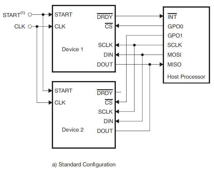
            I want to use two ADS1299 for capturing 16 channels of EEG  signal. So I'm chaining two ADS1299s together as the cascaded mode:  ADS1299 datasheet PDF33.
            
           Master:Arduino uno,only one SPI interface.
    Slave:ADS1299_1, ADS1299_2.
    So I need a GPIO to control the CS1 of Devices2.
           Solution:#define PIN_CS1 (7),I have modified the library of ADS1299.
     
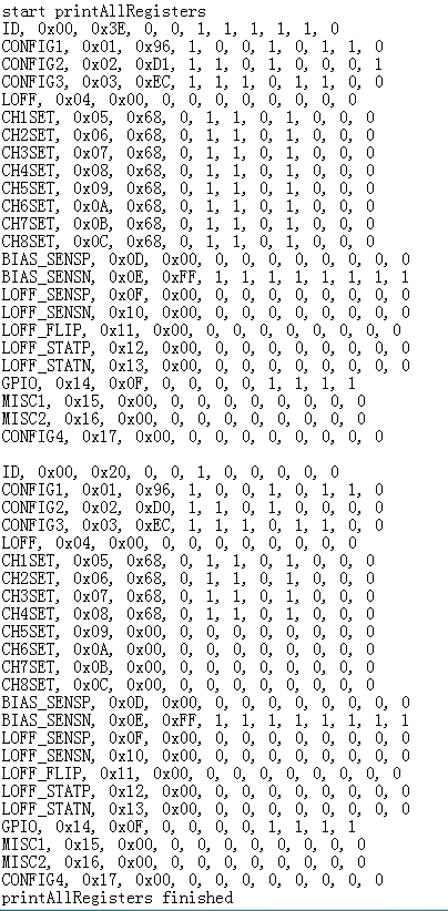
        Running……as we can see the result from the serial monitor:
     
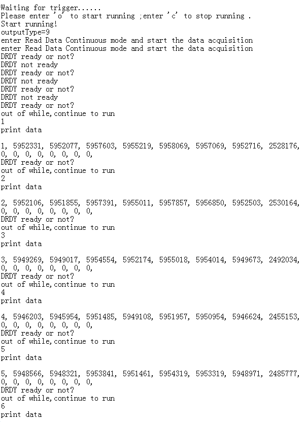
        The value of registers of AD1 are normal,and I can receive the corresponding data of 8 channels.
        The value of registers of AD2 are abnormal,and I can not receive the corresponding data of 8 channels(all Zero).
     
        There are some thing wrong with it,but I do not know why.
        Here I have several questions to ask you.
        (1)As we can see from the first picture of my post,the DRDY pin of Device2 is floating,how can it be synchronizing with Device1 ?By START singal? I do not understand the meaning of Figure39,on ADS1299 datasheet 32.
        (2)It says,when using multiple devices,the devices can be  synchronized with the START signal(ADS1299 datasheet 32). And to set the START pin low and use the START serial command to synchronize and start conversion(ADS1299 datasheet 33),it means I need to set the START pin low,at the same time, I also need to use the serial command,am right?
       (3)Should i set the CLKSET pin =1 and set the CLK_EN register bit to '1'? Should I ? I am not very clear about the  multiple device configuration(ADS1299datasheet 31).It is just about the setting of daisy-chain or it is about all of the multiple device?
       (4)To cascaded mode of ADS1299,any other places I need to set up ? Or maybe something wrong with my program?
       Thank you for having read my message so far and thank you even more for giving me any answer.