This thread has been locked.

If you have a related question, please click the "Ask a related question" button in the top right corner. The newly created question will be automatically linked to this question.

How to return the conversion result from a ADS8317, need C code assistance

Other Parts Discussed in Thread: ADS8317

 Hello

I'm trying to write a SPI function in C language that starts a 16 bits conversion on a ADS817.

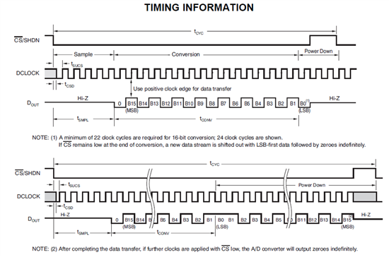
According to datasheet 22 clock edges are required :


Here is the code i've wrote so far :

unsigned int ADS8317_read(void)
{
unsigned char Dummy;
unsigned int ADC_result;

 /***********************************************************************/
 // Configure SPI
 ADS8317_SPIEN = 0;     // Disable the interface

 // Apply new SPI settings for ADS8317
 ADS8317_SPISTATbits.CKE = 1;        // Transmit data from active to idle clock state
 ADS8317_SPISTATbits.SMP = 0;       // Input sampled at middle of data output time
 ADS8317_SPIEN = 1;                           // Enable the interface
  /***********************************************************************/

 ADS8317_CS_IO = 0;            // Enable CS
 ADS8317_SPI_IF = 0;           // Clear SPI Flag

 /*********************************/
 ADS8317_SSPBUF = 0x01;                                       // Send dummy value (0x01) in order to get the FIRST 8 bit byte
 while(!ADS8317_SPI_IF);ADS8317_SPI_IF = 0;   // Wait until data is shifted out
 Dummy = ADS8317_SSPBUF;                                 // Get the FIRST 8 bit byte ( 8 clock edges )
 /*********************************/

 /*********************************/
 ADS8317_SSPBUF = 0x01;                                      // Send dummy value (0x01) in order to get the FIRST 8 bit byte
 while(!ADS8317_SPI_IF);ADS8317_SPI_IF = 0;   // Wait until data is shifted out
 Dummy = ADS8317_SSPBUF;                                 // Get 8 bit byte ( 8 clock edges )
 /*********************************/

 /*********************************/
 ADS8317_SSPBUF = 0x01;                                       // Send dummy value (0x01) in order to get the FIRST 8 bit byte
 while(!ADS8317_SPI_IF);ADS8317_SPI_IF = 0;   // Wait until data is shifted out
 ADC_result = ADS8317_SSPBUF;                          // Get 8 bit byte ( 8 clock edges )
 /*********************************/

 ADS8317_CS_IO = 1;            // Disable CS

 /***********************************************************************/
 ADS8317_SPIEN = 0;     // Disable the interface

 /***********************************************************************/

 return ADC_result;
}


Here i send 3 x 8 clock edges to the chip in order to get the conversion result on MISO line.

For test purposes, V+ voltage is 2.41V and V- pin is grounded.

ADS8317 returns a 3 bytes value but i don't know how retrieve this result  (ADC_result) and return it into an integer.

Can someone show me how to proceed please ? 


How could i verify that ADC_result value is correct according to V+ pin voltage ?

I wondering the following, but i'm not sure this is correct :

ADC_result = ( 32768 x V+ ) / Vs

Vs supply voltage is 3V.

if V+ = 2.41

ADC_result should be ~= 26208.

Do you confirm this calculation is correct ?


Many thanks for your help and advices.

Best regards,


  • Hello Laurent,

    The full-scale input range of the ADC is set by the reference voltage you are using. In particular, -Vref <= Vin <= +Vref. The corresponding output range is -32767 <= output code <= +32767. For your reference, table 1 and figure 44 of the datasheet provide clear illustrations of how the ADC input voltage range maps to its output code range.

    With regard to your particular case, VIN = IN+ - IN- = 2.41V. If you are using a 2.5V reference voltage, notice that your input is closer to the positive end of the input range (+2.5V) than the negative end (-2.5V). So you should expect an output that is closer to the positive end of the output range as well, i.e, something close to +32767 (0x7FFF).

    In order to calculate the exact output code, the "LSB size" of the ADC needs to be computed as follows:

    LSBsize = full-scale input range/total number of output codes = (2.5V - (-2.5V))/2^16 = 76uV/code

    Therefore, the output code for a 2.41V input should ideally be int(2.41V/76uV) = +31588 (0x7B64). From your plot, it appears that the ADC output is 0x671C (+26396) (considering MISO over 16 rising SCK edges starting with the 7th rising edge that occurs after the falling edge of /CS). The output error is over 5000 codes which is much larger than the max combined offset error, gain error, INL and DNL of the part (which is not more than 50 LSB). Please make sure you are operating the ADC according to datasheet recommendations and that your input and reference sources are precise and remain stable even during conversion.

    Best Regards,
    Harsha

  • Hello,


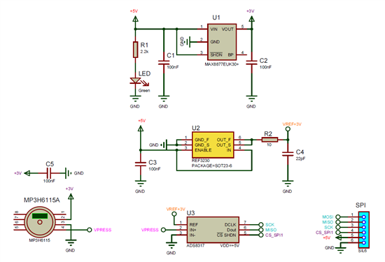
    I use the following schematic and SPI code below :

    The voltage reference used is +3.00V


    I consider the following calculation : V+ = Vpress = ( ADC / 32768 ) x Vref

    I think i could have made a mistake in the code source because i can't get a correct returned ADC value.

    When sensor outputs 2.416V, i should expect to get ADC value =(32768*2.416) / 3.00 = 26389

    The SPI code returns an ADC result about 401 ADC steps less than expected.

    Would you please confirm the following way to return ADC value is correct according to my schematic ?

    Many thanks for your help and support.

    unsigned int ADS8317_read(void)
    {
            unsigned char SPICON1Save;
    	unsigned char SPISTATSave;
    
    	ADS8317_CS_IO = 0;        				// Enable CS
    	ADS8317_SPI_IF = 0;       				// Clear SPI Flag
    
    	/*********************************/
    	ADS8317_SSPBUF = 0x00;					// Send dummy value (0x00) in order to get the FIRST 8 bit byte
    	while(!ADS8317_SPI_IF);ADS8317_SPI_IF = 0;              // Wait until data is shifted out
    	byte1 = ADS8317_SSPBUF;
    	/*********************************/
    
    	/*********************************/
    	ADS8317_SSPBUF = 0x00;					// Send dummy value (0x00) in order to get the FIRST 8 bit byte
    	while(!ADS8317_SPI_IF);ADS8317_SPI_IF = 0;              // Wait until data is shifted out
    	byte2 = ADS8317_SSPBUF;
    	/*********************************/
    
            /*********************************/
    	ADS8317_SSPBUF = 0x00;					// Send dummy value (0x00) in order to get the FIRST 8 bit byte
    	while(!ADS8317_SPI_IF);ADS8317_SPI_IF = 0;              // Wait until data is shifted out
    	byte3 = ADS8317_SSPBUF;
    	/*********************************/
    
    	ADS8317_CS_IO = 1;        				// Disable CS
    	ADS8317_SPIEN = 0;					// Disable the interface
    
    
            ADC_result=(byte1&0x03)*65536UL;           // masked for two LSBs only
            ADC_result|=byte2*256UL;
            ADC_result|=byte3;
            ADC_result>>=2;                                         // Final shift drops unwanted two LSbs of third byte
    
    	return ADC_result;
    }