This thread has been locked.

If you have a related question, please click the "Ask a related question" button in the top right corner. The newly created question will be automatically linked to this question.

ADS8422 ADC nRD timing

Other Parts Discussed in Thread: ADS8422

Hi,

In the ADS8422 ADC, can I tie the nRD pin to ground and just use the nCONVST to do the actual clocking?

Does the nRD pin have to be clocked as well to shift out the data?

I'm trying to minimize the interface pin count.

If that won't work, can I tie the BUSY pin to nRD so that it essentially asks for data automatically when it's ready?

The data sheet has some details about the "quiet zone". Is it wrong to violate the quiet zone in terms of nRD timing (as it probably would when connected to BUSY) as long as I make sure I ignore the data values present till it's outside this zone?

I essentially want to have 8 data lines and 1 clock (nCONVST) driving the ADC and making sure that the FPGA respects the timing requirements for data ready.

Thanks!

  • Hi,

    You can tie the nRD pin to ground and use the nCONVST as you have described. nRD does not clock out data. It is ORed along with nCS to work as a data output enable. If both nRD and nCS are tied to ground, data will appear on the data lines as soon as it is available.

    However, please note in order to collect the 16-bit data on 8 data lines, you will need toggle the BYTE pin as described in the pin description on page 7 of the ADS8422 datasheet. BYTE will have to be set to 1 to cause the LSB byte to appear on DB15..8 pins.

    In order to achieve best performance, no digital interface signals should toggle during the quite time zone. So BYTE should not be toggled during the quiet zone and this in turn would also cause the DB15..8 pins to change states (in td5=20ns max).  

    Ideally, the FPGA should monitor the BUSY signal, which goes low 5ns after DATA(N-1) is available on the DB pins. Once it has read the MSB, the FPGA should set BYTE=1 (outside the quiet zone), read the LSB and the BYTE returned to 0 to wait for the next BUSY low transition.

    If you do not want to connect BUSY to the FPGA, the entire sequence can be controlled from the FPGA. Set CONVST=0, read the MSB byte of the previous conversion from DB15..8, set BYTE=0 after the tq2 has elapsed, read LSB byte from DB15..8 and set BYTE=1 before t(CONV)=180ns. The min nCONVST period (tp1) and min nCONVST widths (tw1 and tw2) specs need to be adhered to as well.

    Regards,

    Sandeep

  • Hi,

    Thanks for the reply.

    I have done a preliminary check to see if I can interface my Compact RIO FPGA system to the ADC and for now I'm using all the interface signals. (I will cut it down later by tying to GND etc when I know that it's working properly)

    I think I can get the data to the FPGA, but the timing seems to be much slower than the data sheet spec.

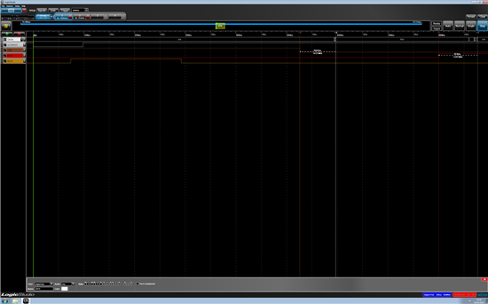
    I have attached a logic analyser screenshot. In that, I trigger off the nCONVST falling edge.

    There are 2 cursors that I've marked. The 1st one is 'td4' and the second is 'td5'. But as you can see, the times are a lot larger than the specified characteristics. (~70 ns vs ~20 ns)

    Do you know why it's so?

    Thank you,

    Kalhana

  • Ok, I figured out the reason for the longer than expected delay in the data ready from nRD and BYTE assertions.

    My ADC is connected to two ADUM1400CRWZ and a ADUM1401CRWZ digital isolator and those chips have a propagation delay of 32 ns. My logic analyser was hooked to the FPGA side of the isolator. Therefore when I assert nRD or BYTE, it takes 32 ns for the signal to reach the ADC, and another 32 ns for the data to come through. This adds a total of ~64 ns and when coupled with the 20 ns of the ADC, explains the ~70 ns observed. (This is the theory, although I haven't bothered to check the actual delay of the isolators vs the 32 ns stated in the data sheet)

    I have followed your advice and tied nRD to GND. I clock the nCONVST and follow the quiet zone guidelines when toggling BYTE. I have opted to ignore BUSY as my target conversion rate is <500kSps and I can afford to wait long enough and assume BUSY is low.

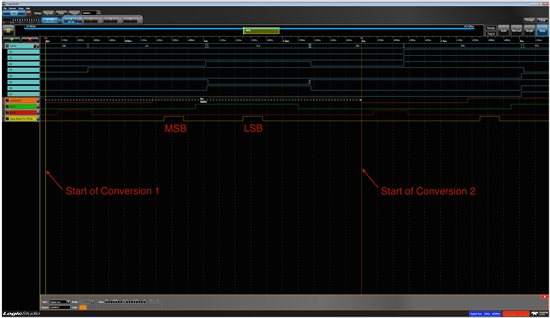
    This way, I only need 10 signals for the interface (8xData, nCONVST, BYTE). I have attached the latest screenshot of the logic analyser. I have added a signal called "Data Read To FPGA" just to see when I do the actual reads. Of course using this method, it's possible to run it faster than the 500kSps I have tried. (It will be limited by the propagation delay)

    Thanks for the advice!

    Kalhana