This thread has been locked.

If you have a related question, please click the "Ask a related question" button in the top right corner. The newly created question will be automatically linked to this question.

TLC3578 channel 7 conversion output error!

Other Parts Discussed in Thread: TLC3578

hi,


Only channel 7  conversion output value is always  wrong.

The remaining channels are the differences are very small.

but channel 7 is  small less 0x18 then other channels. even all channel's is opened.

if you have experience about this issue then help me please!


  • Hello,

    I have a question from customer.

    >Application : Data converter board for Semiconductor equipment

    >part : TLC3578 (5ea/1bd)

    >Problem issue :

    A0~A7(AIO1~AIO8) and Only A7(AIO8) data value is low 0.02~0.04V compart of other channel..

    We have total 40ch and problem port is AIO8,AIO16,AIO24,AIO32,AIO40.

    And VREF_ADC1, VREF-ADC2 is 4.0V.

    Please review of schematic and send me your comment.

    Best regards,

    Eddy Lee(eddy.lee@avnet.com)

    7002.DCS AIO_ES3_201408014(회로도).pdf

  • Hi Eddy,

    Before digging into the details of the problem, I have a few concerns about the reference signal path on this board that are important to address. The fact is that proper load regulation of the reference voltage is critical for ADC accuracy, and certain aspects of this design are not suitable for proper load regulation.

    Load regulation is a function of load current and source resistance - in this case, the load current into the ADC REF pin (which can instantly change from 0 to tens of mA) and the output impedance of the REF signal source which consists of the op amp buffer and bypass caps. Naturally, load regulation degrades (i.e. VREF error increases) if the load current or the magnitude of the source impedance increases. Since the ADC load current cannot be controlled, the best strategy is to make the REF source impedance as low as possible to minimize VREF error.

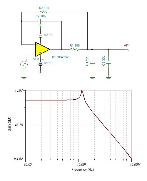
    In this case the ferrite beads (FB1 and FB3) are in the path of the ADC reference load current and add to the source impedance. I would recommend uninstalling FB2 and replacing FB1 and FB3 with jumpers. Direct cap loading from the 3x(10uF + 1uF + 0.1uF) will probably cause the op amp to become unstable. Simulation shows >>1dB peaking in the closed loop gain response of the circuit.

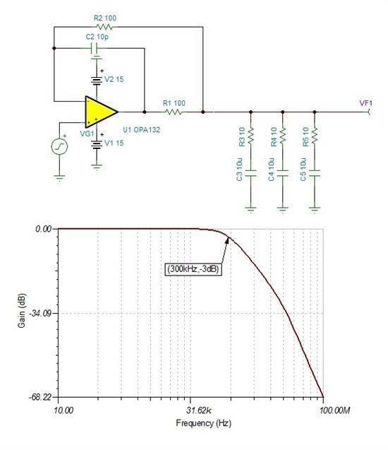
    I would recommend uninstalling the 22uF caps (C105, C91), as well as the 1uF and 100nF caps on each ADC REF pin. In addition, 5-10 ohms of ESR will probably need to be added to each 10uF cap at the output of the REF buffer for isolation without increasing source resistance.

    Best Regards,
    Harsha