This thread has been locked.

If you have a related question, please click the "Ask a related question" button in the top right corner. The newly created question will be automatically linked to this question.

ADS1247 offset problem

Other Parts Discussed in Thread: ADS1247, LMZ14201, LM1117, ADS1220

Hello,

I'm using an ADS1247 to measure two analog signals on AIN0-1 for the first and on AIN2-3 for the second ! It works well and I can read value precisely near 0V without any offset ! But sometimes, when I switch off/on the power supply, suddenly there is an offset of about 13mV between the result read from the ADS1247 output register and the real voltage present on the AIN pins ! It seems to be a threshold because if the voltage present on the input pin stay between 0 mV and 13 mV, the output register always give 0 ! And if the voltage rise up above the 13mV the output value follow it with the permanent offset !

So, firstly, I thought that it was a problem with the selfoffset calibration command ! I checked the content of OFC registers with and without the problem offset ! It has always about the same value in it ! So the problem is not here ! I tried to force the OFC to 0 and the problem always appear : sometimes perfect, sometimes with offset !!

So, finally, I tried to measure the reference voltage on Vrefout/Vrefcom, and I noted that when it works without offset problem, the voltage between Vrefout/Vrefcom is 2.048V and when the 13mV offset problem appear, this voltage drops to 2.032V ! It seems to be linked !

But I cannot understand why the reference voltage is different from time to time !

So I use the ADS1247 internal voltage reference and I connected the Vrefcom pin to GND with short path and add a 10uF tantale capacitor between Vrefout and Vrefcom as described in the datasheet !

So I don't know what to do now ! Is somebody know that problem and could help me ?

Thank you in advance !

Maël Vallat

  • So, I noted another interessant thing ! When the offset error is present, I just cool the ADS1247 and the offset error disappear instantly ! Then I switch off/on the power supply and the offset error is present again !

  • Maël,


    I've never seen behavior like what you describe in your post. To help answer this question, I need a bit more information. I'm guessing that you are running the device in a gain of 1, using the on-board reference, but what are the other settings? Is this a board that you designed and what type of device are you measuring? I'd like to know more about the system that you have put together.

    What is your power supply? Is this part of your system or a variable DC power supply. What voltage are you operating at. What other devices do you supply with this power supply? Does the problem appear only when powering on and off the device?

    Do you load the reference of the device with any circuitry? When you measure the reference do you measure the output from REFOUT to ground a the pins of the device? There may be some ground loop currents that may be affecting your measurements.

    Are you measuring AIN0 and AIN1 close to the pins? Is the negative input connected to ground in a way that may have ground loop problems?

    You mention that the offset disappears when you cool the device. Is the device running hot?

    I'll wait back to hear from you, and we can see what debugging we can do.


    Joseph Wu

  • Joseph,

    Thank you for your reply !

    So, about the settings :

         - Burnout current source --> OFF

         - Positive input --> AIN0

         - Negative input --> AIN1

         - Bias voltages not enabled

         - Internal voltage reference is always ON

         - Onboard reference selected

         - System monitor --> Normal operation

         - PGA = 2

         - DOR = 10 SPS

         - Excitation current source DACS IMAG --> OFF

         - Two IDACs --> disconnected

         - All the pins are used as analog input --> GPIOCFG = 0


    Yes, it's a board we designed for our application which has to measure the voltage on a shunt ! So, the type of device we measure is simply a shunt voltage amplified by an AD706 ampli-op used as inverser amplifier !

    On the second pair of inputs (AIN2-AIN3), we have also a simple voltage provided by the output of an other AD706 used as follower !

    About the power supply : We use a voltage of 3.3V provided by a LM1117 linear regulator ! It's a part of our system ! Our board is powered by a 15V DC and we create firstly a 5V supply with a LMZ14201 and then a 3.3V supply from the 5V with the LM1117 ! We need the 3.3V for the SPI level communication with our microcontroller !

    The 3.3V supply the microcontroller ATXMega64A3U too

    The problem appear at the power on and always stay until we power off or we cool the ADS1247 !

    About the ADS1247 voltage reference : We don't use this output for anything ! There is just a tantal capacitor of 10uF between Vrefout and Vrefcom ! When I measure the voltages with multimeter, I always measure on the pins of the device ! The ground is a plane on one side of our PCB !

    The device isn't hot, but when we spray a cooling product, the offset disappear !! It's crazy ! I d'ont understand !


    Thank you for your help, I hope we will find the problem !


    Maël Vallat

  • Here is the schema we use !

    I just want to specify that, when we spray some cool product on the ADS1247 chip, the offset error disappear and never come back until we switch off the internal voltage reference, we wait for about 5 sec and then we switch on the internal voltage reference again !

    So with our experiment, we discover that the offset error appear after we make the following actions : 

        1. we switch off the internal reference voltage

        2. we wait a delay of about 5 sec

        3. we switch on the internal reference voltage again

    Then to remove the offset error we have to spray some cool product on the ADS1247 !!

  • Maël,


    It looks like the problem is that AIN1 and AIN3 are outside the input common mode range. There are a wide variety of problems that can happen when the inputs are outside the usable range. In the datasheet there is a specification shown here:


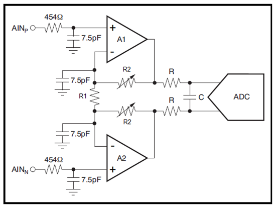
    The input for the ADS1247/48 is set up like the front-end of an instrumentation amplifier. There are two amplifiers with feedback that sets gain with a set of resistors. It's described in the Low-Noise PGA section on page 26 of the datasheet and it's best illustrated with Figure 53:


    In gain of 2, the inputs still need to go through the amplifier and you are limited by the resistor divider going from the output of A1 to the output of A2. Think of it such that the voltages at AINP and AINN are put onto the negative inputs of A1 and A2. Then the A1 and A2 set the outputs to give gain.

    At this point, I think the only thing you can try to do is to lift the pins to AIN1 and AIN3 to disconnect them from the ground. Then reconnect them to some other common mode input voltage. REFOUT might be a good common-mode reference point depending on expected input voltages.

    If you need some other device, the ADS1220 has a little more noise but can cover the input range all the way to ground - even in gain.

    Joseph Wu

  • Looking back over the ADS1220 datasheet, you'd still need to either use G=1, or use G=2, but be careful over the input of what you are measuring because the PGA gain may still interfere with measurement at input ground.

    Joseph Wu

  • Joseph,

    Thank you for your reply !

    So, I tried to completely disconnect the AIN pins and activate the Voltage Bias on these pins ! So the voltage on the AIN pins is 1.65 now ! I measured them with a multimeter ! So we are ok with the common mode voltage limits ! I configure the PGA = 1 !

    So in these conditions the offset problem must not appear, is it ?

    But when I read the output measure register, the same offset problem is always present !!

    It seems to be very strange !

    Thank you for your help

    Maël Vallat

  • Maël,


    First, I would not use the VBIAS line as an input for measurement in this application. It's simply a divided down version of the supply voltage and it's likely a very noisy source for measurement. It should only be used as an input as a bias for unbiased thermocouples because any noise on VBIAS would appear as a common-mode noise. There, any noise on AINN is also coherently seen on AINP so that the noise cancels out. In your system, the noise on AINN is additive because it is not the same noise on AINP because your measurement comes from some other source. Also, the AVDD/2 value is generated from some buffered resistor divider and the error associated with that value may be large. You cannot guarantee that the value is exactly 1.65V. I suggested the REFOUT line to ensure that this is a clean input and well defined.

    On another point, I had suggested that the AIN1 and AIN3 lines are outside the input common-mode range, but I neglected to mention that you should also ensure that the AIN0 and AIN2 lines are also not outside the input common-mode range also. I'm not sure this is the case, but it seems that this is still possible.

    Let's look at the AIN0 measurement from the AD706 (pins 1, 2, and 3). Assuming there is no current in the shunt measurment, The input to the amplifier is 0V. That gives 0V out and another 0V at the AIN0 pin, which is also at 0V. Once again this outside the common mode range. I don't know positively that you're measuring a shunt current with this amplifier, but if the input voltage (on R7) rises, the output voltage falls because the amplifier is in an inverting configuration. That would make the input even more negative at AIN0.

    I would first confirm that this is the case. I would power up the device and measure AIN0-AIN3 referenced to ground (in your case MES). If any of them are less then 100mV, then you are outside the input range of the device. Then measure the voltages across C13 to measure REFOUT. Also measure MES Iout (and calculate what voltages you expect from it). What input range do you expect for the AD706? Is current being shunted into or out of Shunt_4?

    If you are outside the input range, you might be able to get a reading by expanding the input range. First set AIN1 and AIN3 back to the original ground (MES). Then you could construct a different supply voltage for the ADS1247 analog section. If you connect AGND (pin 13) to -0.5V (that you would need to generate), AGND to VA+ would go from -0.5V to +3.3V. That way, the analog input range for AIN0 to AIN3 becomes -0.4V to +3.2V as long as you are in a gain of 1. Note that you may need to connect a small capacitor from -0.5V to REFCOM for stability of the reference. Leave DGND at 0V (the MES level) so that the digital communications aren't affected. If you are in a gain of 2, you may need to lower VA+ and AGND to makes sure the analog inputs are still in range.

    Let me know if this helps, if you continue to see the offset problem, then we'll have to start probing more nodes in the schematic, and get more details about the input signals that you are measuring, with more of the schematic.


    Joseph Wu

  • Joseph,

    Ok, I was not clear enough in my last reply, sorry for that !

    So, I used the VBIAS only to test if the offset default always appear even if I removed the common mode input range problem ! I will not use it for my application !

    So, for that test, I completely disconnected physically the AIN0 and AIN1 inputs and I activate the VBIAS on that 2 inputs ! So, I now have about 1.65V on these two inputs. Then I select these two input for the conversion by the mux registrer. So, in these conditions the common mode input range is respected, isn't it ? I normally have to measure a value near to 0 because the differential voltage between the 2 inputs is about 0V !

    I can observe that the offset problem is always present ! I measure about 2000 in the ouput register, and when I spray some cool product on the ADS1247 chip, it suddenly drop at 0 ! And then it keep that value (with some variation due to noise, of course) ! I have to switch off and switch on the power supply to measure about 2000 again !!

    In conclusion, the offset default don't come from the outside of the common mode input range !

    And this test is completly independant of our analog part of the schema because it is not connected to it ! It is a problem inside the ADS1247


    Thank you for your help, I hope that we will find a solution because we are very pleased about the rest of the fonctionality of the ADS1247 ! And it is urgent for us to find a solution because we have produced a lot of device before that problem suddenly appear !


    Best regards


    Maël Vallat

  • Maël,


    I still think that you're violating the input common mode range on this part. Let's just use your example, where the negative input is set to 1.65V, but the positive input is set to 0V. This sets the input common mode to 1.65V/2 or 0.825V.

    Going to page 26 of the datasheet, this common mode input must be within the range of shown in equation 4:


    The upper bound is not going to be a problem. Look at the lower bound of the equation. AVSS+0.1V+(VIN)(GAIN)/2 is the lower bound. Assuming the GAIN is 1, we have the largest range possible. Plugging in GAIN=1, VIN=1.65V, and AVSS=0V, we get a lower bound of 0V+0.1V+(1.65V)(1)/2 = 0.925V. This is the lowest value the common mode input should be while the input is 0.825V.


    I had included a figure of the ADS1247 PGA to illustrate this. However, I'm including another to show a little more detail.


    The thing to keep in mind is that the input to A1 and A2 should never be below AVSS+0.1V. Normally, the voltage on AINP is impressed on A1's negative input and the AINN is impressed on A2's negative input. This puts a voltage across R1, then A1 and A2 drive the current through both R2 values so that R1's voltage reflects the input. Then the output of A1 and A2 give the gain (which becomes (R1+2*R2)/R1). In gain=1, R2=0.

    All this works as long as the op-amps behave correctly. However, when the inputs are outside the input range of the op-amp, or when the output of the op-amp is too close to 0V, this breaks down and the input PGA fails to operate.

    It's possible that the freeze spray alters the exact value of the input range of the op-amp, or that the output voltage of the op-amp can be driven closer to 0V. However, I'm still pretty sure that the input common mode range is still being violated.

    I'm checking to see what the PGA will do when the common-mode range is violated to see if it matches what you're seeing, but until I find out for sure, check your input values to makes sure that I haven't made a mistake.


    Joseph Wu

  • Joseph,

    Thank you for your reply !

    Ok, I understand your explanation very well, it's clear !

    But in my test case I set the positive input AND the negative input to 1.65V !

    So, AINP = 1.65V ; AINN = 1.65V --> Input common mode voltage = 1.65V

    And VIN = 0V in this case !

    So, the lower bound is now 0.1V !

    So, we are not violating the common mode voltage range !

    But the offset problem always appear in this configuration !


    Maël Vallat

  • Maël,


    After reading through the correspondence, I'm still not sure what the problem is. Since I'm still a bit unsure what we've covered, it might be best best to make some measurements on the device with a multimeter.

    Starting with the last set of measurements you made, you said that the input AIN0 and AIN1 set to VBIAS0 and VBIAS1 and you measured 2000 codes for a measurement with normal temperature and 0 codes with cold spray. With GAIN=1, that's still a pretty small value (I think that's just under 500uV). I'll need to make sure that the VBIAS for each of the channels go to the same point to make sure the values should be exactly the same.

    Looking at other things with the same setup, first let's look at the reference. Measure REFOUT to GND, with and without the cold spray. Earlier you mentioned that you had different values. Confirm that with a multimeter.

    Then instead of connecting both inputs to VBIAS, you could run through the MUXCAL settings before and after the cold spray to make sure the values the don't have the same shift. Look at the offset measurement (000), the gain measurement (010), and the temperature measurement (011). I want to see if these internal measurements have the same offset before and after.

    I'll likely try to contact you directly through the email you provided to e2e. It might help if we can exchange more of the schematic (to see if there's other parts that may affect the measurement). Also, a layout of the schematic might help as well.


    Joseph Wu

  • Joseph,


    Firstly, I'm sorry to answer you so late ... But, I was out of my office during one month and I didn't work on that project during this time !


    My colleague told me that he has discovered something very interesting during my absence :

    He tried to change the value of the capacitor connected between VREFOUT and VREFCOM. If this capacitor value is under 3.3uF, the problem described previously never appear anymore !! But if we put some greater values, the problem always appear !!

    Furthermore, the capacitor don't have to be tantale !!

    So, it must be a ceramic capacitor under 3.3uF, if we want no problem !!


    In your datasheet, it is specified that this capacitor value should be in the range of 1uF to 47uF ! So I choose the value of 33uF for my design, but we saw that it didn't work very well ...

    Thank you for your help

    Maël Vallat

  • Maël,


    I'm glad you were able to find a solution. I'd still be worried about your input common mode range as we had discussed, but if you were able to work around that, it should be ok.

    When it comes to the internal reference cap size. It will affect the amount of time it takes to start up and settle to a final value. Table 10 on page 29 of the datasheet describes the tradeoff between settling error and the VREFOUT cap. There should also be a low impedance path of less than 10 Ohms from VREFCOM to ac ground nodes (which in your case should be ok). If you needed to, you could take an oscilloscope photo of the rise VREFOUT to see how long it takes with larger capacitors to verify the length of time it takes.

    Regardless, if you have any other questions, feel free to post back to the forum.


    Joseph Wu