This thread has been locked.

If you have a related question, please click the "Ask a related question" button in the top right corner. The newly created question will be automatically linked to this question.

Layout on small 12-bit DAC7611

Other Parts Discussed in Thread: DAC7611

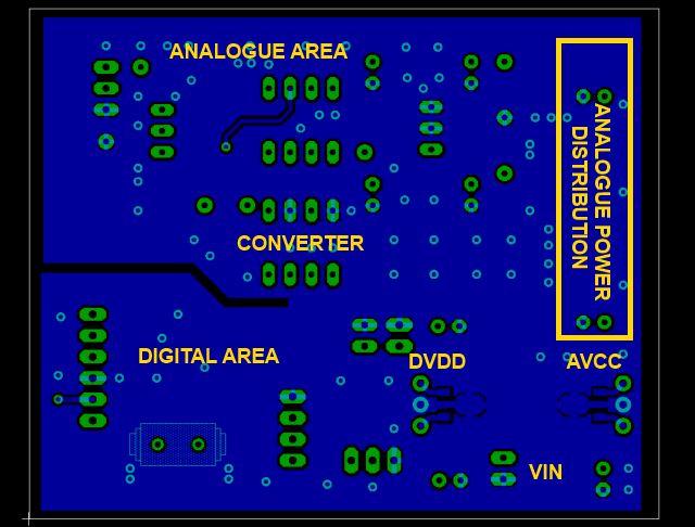
I am considering using this small 12-bit DAC for low speed precision analogue output from a flow gauge (it outputs RS232). Update rate 500Hz max.  All low power, entire thing shouldn't draw more than 30mA max.

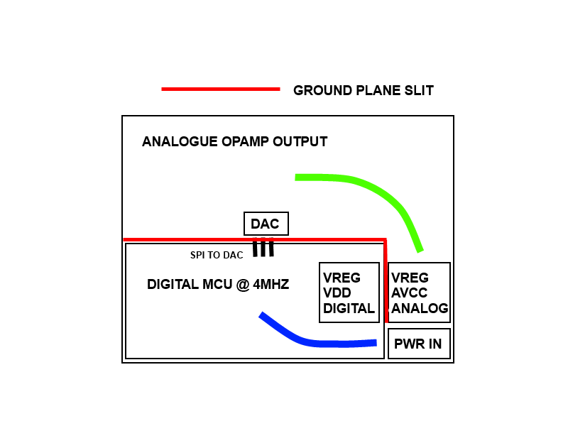
As with almost all mixed signal designs these days, I am still somewhat confused about splitting the ground (or rather adding a slit to separate analogue and digital returns.

With all the wisdom available on the internet many seem to conclude to use a solid ground plane, with analogue and digital components in different area's.  This makes sense, however, many many TI evaluation board designs appear to use separate grounds, joined at one point - be it under/near the converter, or at the power supply.

I have an initial very basic design, but given the SPI (digital) is feeding data to the DAC, the returns from these are from the AGND (DAC only has one ground pin, fair do's) and so must run back through the analogue ground.

Is this a fair layout in terms of resolution? Green and blue are analogue/digital return paths respectively.  As you can see, the input power is used for separate linear regulators, one for digital, and one for analogue. Only lines that cross the ground boundary are the SPI connections.

If I was to join the two ground planes under the DAC, surely the analogue return paths would have to go through the digital side?

Apologies for yet another 'layout' question.  I realize each application is different, but there is much conflicting information floating around.

Scott

  • Hello Scott,


    Usually the topic of ground splitting becomes more significant with higher precision devices with a resolution >12-bit. So I don't think that it will be as critical for the DAC7611.

    With this 12-bit device I would suggest having a single GND plane on the entire board. Place the analog and digital pieces on opposite sides of the board. When there is not a GND split, return currents tend to travel underneath the trace. The physical separation of digital and analog traces should be enough to keep any digital return currents from affecting your analog lines.

    If you are still interested in using a split plane because of other sensitive circuitry on the board, connect both GND planes underneath the DAC. Trying to trace over a GND split can cause more harm because of the long and complex return current paths that it creates. If you have any other high precision data converters on board (>12-bit) place it on the split as well.

    Something to keep in mind with any approach: Connect the GND pin to the GND plane as close to the device as possible.

    • Tracing the GNDs to connect them at a single point or "star connect", can cause the GND potentials of each device to be different if the trace lengths are not matched plus a few other effects that I won't mention in the interest of time. I would not recommend this approach.


    If you have any other questions, please feel free to ask.


  • Thank you for the reply sir!

    I did indeed go with a solid ground plane for digital and analogue, with the top half of the board dedicated to analogue, and the bottom half for digital.  I realise it is a low power DAC, and the PCB had  only an MCU, DAC, and opamp on board, but it is nice to attempt to squeeze the best out of the layout.

    As per your advice, I checked the return paths for signals, assuming they run under the signal trace for high speed signals, and 'line of sight' for low frequency/DC.  They didn't cross at all, so hopefully circulating digital currents will stay on the digital area.

    I did however add a small slit in the ground. (not ignoring your advice here!). I have attached an image of the bottom layer to show this (the same ground plane is on the top layer too, but interrupted by many signals).  This is a test board for another DAC, but the same layout has been done for the TI part.   I was thinking that low frequency currents *may* circulate across the area's in that location, so the slit was added - no traces cross this boundary, or have had to be rerouted, it was just plane.  It does seem to be bad practice to add any slits, and I was probably wrong to add this, but I made sure it obeyed the rules that you stated. (return paths not interrupted, no traces over slit).

    Once the boards arrive I shall try and borrow 'the good test gear' for some noise/accuracy results. I never expect the 'best' measurements stated in the datasheets - but as close as possible is good :)

    Thanks again,

    Scott