This thread has been locked.

If you have a related question, please click the "Ask a related question" button in the top right corner. The newly created question will be automatically linked to this question.

RTD measurement using ADS1248 : Accuracy issues during long run

Other Parts Discussed in Thread: ADS1248, TIPD120, TPD4E110, ADS1262, ADS1220

Hi all,

We have designed a RTD measurement system, using 24 bit ADC ADS1248 from TI. 

We are measuring different RTD types like Pt100, Ni100, Pt200 , Pt1000 etc. Maximum resistance we need to measure is around 3.9KΩ. Thus we have used a high precision 4.3KΩ as RREF & IDAC out to be 500uA in our design.

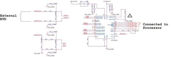
Below is the snapshot of the RTD measurement section of the schematics.

We are able to measure the resistance & calculate the temperature as expected using the above design.We are  calibrating the entire system at the beginning. We are achieving good accuracy with this method.  

Only issue we are facing is with respect to the accuracy of measurement during a long run. If we connect a constant  resistance for a long period of time, we are observing significant variation in the ADC readings.

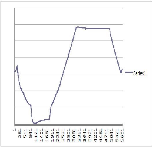
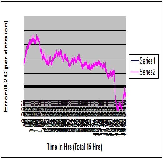
For example, we are simulating a constant resistance of 3901.9Ω using a RTD simulator. If we keep our system running with this resistor for 15 hours we are observing around 3Ω variations. This corresponds to around 1°C variation with  respect to Pt1000 RTD.

Below is the plot of variation in°C with respect to time. 


RTD simulator we are using is having a accuracy of 0.4Ω. We are not able to find out the reason for 3Ω variations in  reading over the long run.

Is there anything we can change in our design to avoid this variation ? Please suggest.

Thanks,

Suresha N S

  • Suresha,


    I've looked over the schematic and don't see anything wrong with the schematic and the way you have it set up. There are only a few things that we can see that might be problematic I'll just go through them to see if they are applicable.

    First, I'd remove the filter that you're using for AVDD. Often, if there is inductance, it may cause large voltage spikes because of the periodic current load because of the digital switching internal to the device. This may be more of a concern for the noise or reference accuracy than anything else, but it's still a concern.

    The schematic you show has an ADC_IOUT connection, but it doesn't show where it goes. I'd like to know what other circuits are connected to the RTD simulator. If there are protection diodes, there may be added leakage current that add error to the measurement.

    Also, what type of capacitors are you using on RTD0_P to RTD0_N and for REFP and REFN? Often, we use C0G capacitors for the best performance. Other lesser grade capacitors may have some piezo effect that contributes noise translating vibration into electrical signal. This is more of a noise effect, but if there is a long term stress on the board, it might be seen as a shift.

    What model resistor are you using for the reference resistor? I want to make sure that these have both the accuracy and temperature drift necessary for the application.

    What RTD simulator are you using? I'd like to see what the specifications are on the device. Also, what is the length of wire you use to connect it up? Since it seems you use a two-wire measurement, the series resistance is also a factor.

    Is the device kept at a constant temperature over this time period? Are there any other long term drifts associated with your tests?

    Let me know if you have any follow up questions, but look through my comments and see if any are applicable to you.


    Joseph Wu

  • Joseph,

    Thanks a lot for your suggestions.

    Please find the clarifications below:

    1. We have removed filter present on AVDD line as per your suggestion. We have kept the setup for long run testing. 

    2. I missed out to include the analog switch part of the schematics. Please find the schematics below: 

    Even though analog switch has its own ON-resistance, we think this will not be issue since we are using a constant current source.

    3. We are using C0G grade capacitors in filter circuits. Reference resistor we are using in having 0.05% tolerance & temperature co-efficient of 10ppm/C.

    4. We are using RTD simulator model 4420 from Burster. I have attached the specification document of the same.

    5. We are using 3 wire RTD measurement mode to cancel out wire resistance.

    6. We did not observe any significant board temperature change during testing period. We have measured the temperature using a temperature sensor.

    Please let us know your thoughts about above points.We will let you know the results of tests with filter on AVDD removed.

    Regards,

    Suresha N S

    4420_EN.pdf
  • Suresha,


    What analog switch are you using? It's not specified in the schematic. It is possible that the current leakage from the analog switch is part of the problem.

    Also, how do you have the excitation current routed through the RTD? It looks as if you have it routed through RTD_O at one point, but also there's a connection to RTD_P.


    Joseph Wu

  • Hi Joseph,

    We are using Quad SPDT ADG1434 as analog switch. We are using Quad SPDT since we have two RTD inputs. ( In the schematics, we have included only one RTD input ).

    This analog switch is used to connect the ADC_IOUT pin of ADC to either "P" terminal or "O" terminal of connected RTD. This connection is controlled by the GPIO's present in the ADC.

    Below is the sequence we are following for a 3 wire RTD measurement : 

    1) Connect ADC_IOUT to GEM_RTD_P_1 

    2) Measure the voltage Vadc1 across RTD0_P & RTD0_N

    3) Connect ADC_IOUT to GEM_RTD_O_1

    4) Measure the voltage Vadc2 across RTD0_P & RTD0_N

    5) Calculate Vadc = ((2*Vadc2)-Vadc1))

    6) Calculate Resistance = Vadc / Excitation Current (500uA)


    Measuring voltage twice will help us to achieve accuracy equivalent to that of 4-wire RTD.


    Meanwhile, we have performed long run test after removal of filter on Avdd supply. We are not observing any improvement with respect to accuracy. 

    We have also tested with high accuracy fixed resistors, and we are observing same kind of variations with that also. 

    Thus we feel the issue is with our design, but we are unable to find out the exact reason.

    Please let us know your thoughts on the design & how we can improve the accuracy. 

    Thanks,

    Suresha N S

  • Suresha,


    Is it possible for you to report back the measurments of Vadc1 and Vadc2 separately? I would plot the values for Vadc1, Vadc2, and your ((2*Vadc2)-Vadc1) separately. I want to see if any of these measurements are cleaner than the other two. I'm not sure I understand the reasoning behind taking two times Vadc2 and subtracting Vadc1, but I can't see how you have the RTD connected, for each of these conditions.

    How long is there between the Vadc1 and Vadc2 measurement? With the switch, there may be some time where ADC_IOUT may not be flowing and either the reference or the analog input may not be settled.

    Another thing I noticed was that the analog switch is not specified for +5V operation. It's specified for +/-15V, +12V, or +/-5V operation. I don't know if there are major changes in leakage current or resistance between channels, but it might be a factor. Is there a way to get this to a specified range of operation, by increasing the supply to +12V?

    One thing to try would be to use a direct measurement of the RTD and the reference with a precision multimeter (like an Agilent 34401A or 3458A). Perhaps making a similar measurement once every 30 minutes of the RTD and the reference voltage. While the accuracy may not be the 0.1% that you're looking for, the linearity of the measurement should capture the change in gain error over time that you are seeing. This would verify that the ADC is making a correct measurement based on the input voltage and the reference it sees.


    Joseph Wu

  • Hi Joseph,

    Thanks a lot for your suggestions. It is really helping us to move ahead with debugging. 

    I have attached a document explaining the method we are following for RTD measurement. Let us know your thoughts on the procedure.

    As you suggested, we will try to plot Vadc1 & Vadc2 variations separately. Also, we will try to measure the input voltage & reference voltage using a precision multimeter.

    Since you are suggesting analog switch may be causing some issues, we are also planning to test the RTD measurement with the switch removed & ADC_IOUT directly connected to RTD. Although we will be able to measure 2-wire RTD only with this setup, we should not see any variations in the reading if analog switch is creating issue.

    We will perform these tests & let you know the results.

    Thanks,

    Suresha N S 

    RTD_Measurement.doc
  • Hi Joseph, 

    Actually, in the earlier post, I gave the wrong link for the datasheet for analog switch. The switch we are using is ADG704. Sorry for the confusion.

    We executed some long run tests & below are the observations.

    1) We took Vadc1 &Vadc2 separately to see if any one of the readings has the issue. We found out that both are having same behavior & both graphs match exactly as that of the temperature variation plot.

    2) We had around 100mS delay between current flow & ADC readings in case of both Vadc1 & Vadc2. We increased this to 5sec. But there was no improvement in the performance.

    3) We enabled only one RTD channel in 2-wire mode. This was to make sure that ADC needs to take only Vadc1 without any change in the analog switch position. We observed a highly improved performance with very less amount of variation in temperature readings.

    4) We carried out the same testing as above , but with current source IOUT being turned OFF & ON in between each readings. We got a very good performance with this also.

    Above results reveals that your concerns regarding analog switch was correct. We don't know the reason behind this behavior. 

    We are exploring options to use other switches.

    Can you suggest us any analog 1:4 switch for this application from TI ? 

    Looking forward to your response.

    Regards,

    Suresha N S

  • Hi Suresha,

    Joseph is out of office this week so I try to cover for him. I read through the conversation and would have suggestions on how you could potentially improve your design.

    First of all I believe we can get rid of the analog MUX altogether. You have pins IOUT2, AIN2 and AIN3 left unused on the ADS1248 as far as I can see. The ADS1248 can route the IDACs to any of those pins internally. So you could route a dedicated wire to each of the RTD leads (e.g. IOUT1=RTD_P_1, IOUT2 =RTD_O_1, AIN2=RTD_P_2, AIN3=RTD_O_2) and then control through the registers which pin the IDAC should be routed to.

    Your algorithm to compensate for the lead resistance in a 3-wire RTD measurement will work, but we purposely integrated two matched IDACs inside the ADS1248 to ease the lead resistance compensation. Attached presentation shows the principle of our suggested implementation. With this approach you don't even need to take two readings to compensate for the lead resistance.
    You will have to rearrange the connections of the RTD leads in your design to implement the proposed circuit. If you want to keep your 4.3k reference resistor you would just use an IDAC value of 250uA for each IDAC then and increase the PGA gain to 2 (your code needs to change then as well of course).

    For the 2-wire measurement you could then either turn one IDAC off, set the other IDAC to 500uA and reduce the gain to 1.
    Or you just leave both IDACs on, the 2nd IDAC will then only flow through the reference resistor and do nothing else. That way you could leave the gain setting (and code) the same for both the 2-wire and 3-wire RTD measurement and also would not have to calibrate the system for each case separately.

    Can you tell me how your code to calculate the RTD resistance looks like?
    You should not use the value of the IDAC current itself for the calculation - just the ratio of RRTD and VREF - otherwise your measurement is not really ratiometric anymore.

    Regards,

    3-wire RTD Measurement.pptx
  • I also attach a calculator that I built for ADS1248 and RTD measurements. Hope it is helpful.

    Regards,

    ADS1248 Calculator.xlsx
  • Hi Joachim/Joseph,

    Thanks a lot for your suggestions.

    We removed the analog switch as per your suggestion, but still face the same variation issue.

    Finally, we found out that the variation is due to variation of ADC temperature. We had made some calculation error earlier due to which we thought the error is generated by analog switch.

    To make sure that the issue is with the variation of ADC temperature, we enabled the ADC internal temperature sensor. We found out that the RTD resistance is varying as the ADC temperature changes over a long run. During this testing ADC temperature was varying up to 17°C whereas the resistance varied upto 0.9Ω.

    Using thermal chamber we maintained a constant temperature of 35C & tested over a period of 18 Hours. Here the ADC temperature varied 0.3°C & the corresponding resistance variation was 0.035Ω. This proves that as long as the ADC temperature remains constant, we are able to achieve a good accuracy.

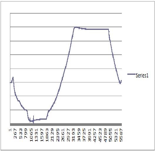
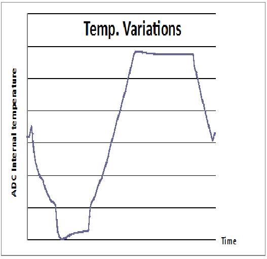
    We have a requirement of 0.3% FSR accuracy over operating temperature range of -20°C to +60°C. Thus we tested the board over this operating temperature range. In this case we observed a 6.9Ω variation in RTD resistance. This corresponds to around 19.3°C of temperature variation when Pt100 RTD is connected. Below are the plots of ADC temperature & RTD resistance measured. This variation is way beyond our requirement.

    ADC internal temperature variations: 

    Measured RTD resistance variations :

    We think in our design apart from ADC, only 4.3KΩ resistor (0.05% , 10ppm/°C) used for reference generation can be the source of error. Thus we think that the majority of the variation in RTD resistance reading is contributed by ADC itself. Is our assumption correct? If so, can you suggest some methods to reduce this variations? 

    Thanks,

    Suresha N S

  • Suresha,

    Can you show the plots with the axes labeled? I'm not sure what it's showing.

    Joseph Wu

  • Hi Joseph,

    Sorry for the confusion. 

    Please find the plots below: 

    Our temperature profile in as detailed below :

    1) Starting temperature : +25°C

    2) Ramp Down : +25°C to -20°C : 20 Mins

    3) Soaking at -20°C : 30 Mins

    4) Ramp up : -20°C to +60°C : 40 Mins

    5) Soaking at +60°C : 1 Hr

    6) Ramp Down : +60°C to +25°C : 20 Mins

    As you can see, both the ADC internal temperature & RTD resistance variations are in line with ambient temperature change.

    Thanks,

    Suresha N S

  • Suresha,


    First, the ADS1248 should have temperature drift of a few hundredths of a percent in gain error through the range of operation. In the datasheet, it's shown in Figures 19 through 22. In general, this gain error drift depends on the skew of the drift of between the sampling capacitors of the input and the reference. That being said, you're still seeing some gain error drift in the measurement.

    I've looked over this thread and I can only think of a few other things to try. Generally, this error shows up only in differences in the sampling of the input to the sampling of the reference.

    One possibility is that the input impedance of the reference is only 500kOhms. With the input filter at the reference input, this divides down the reference by one part in 100. I'd run the test replacing the 3.3kOhms with 0 Ohms instead. If the 3.3k resistors had a large drift it might account for some of the error.

    I'd like to get a plot of the layout to see if there are any other possible sources of series resistance in either the input RTD measurement or the reference measurement. It might also help to know if your 3-wire RTD has a considerable length to it that might add on a large series resistance. If the length is longer, then the additional series resistance could be much larger, with a greater chance of matching error.

    As for the graphs, can you give the y-axes? I've read your description of the temperature changes, but I'm not sure about the second graph of the RTD measurement. I'd really like to see the voltage. Also, is this the RTD measurement? or is it the RTD error? If you can send back the exact values of the results and how the error is calculated.

    Another possible test would be to measure the rtd value and the reference value directly with a precision mutlimeter. That would give a direct measurement of the input and reference that the ADC also measures. Then you can compare the values directly and measure the change in gain error over temperature.

    I know this is quite a bit to ask. Let me know if you are able to test some of these things.


    Joseph Wu

  • Joseph,

    Thanks for your suggestions.

    I have attached excel sheet which we used to plot the graphs. We configured ADC in such a way that ADC will measure the internal temperature diode & external RTD resistance alternatively. 

    Internal Temperature measurement steps:

    1) Vadc = (Value read from ADC * 2.15V / (2^23-1)) ; Here 2.15V is the reference generated when 500uA current flows through the 4.3KΩ resistor. 

    2) Temp = ((Vadc*1000)- 118mV) / 0.405mV  ; Here 118mV is the diode voltage at 25°C. 0.405mV is the temperature co-efficient.

    3) ADC internal Temperature = 25 - Temp in °C

    Since we are concerned about variation in temperature only, we have not calibrated this reading. Thus the actual reading is not same as ambient temperature.

    RTD resistance measurement steps:

    1) Rrtd = (Value read from ADC * 4.3KΩ / ((2^23-1) * PGA Gain)) ; Here 4.3KΩ is the reference resistor we have used in our design.

    We have plotted both ADC internal temperature & RTD resistance variations only. Variation means the difference between the read value and the minimum read value over the entire time period. 

    Can you please verify our calculation once ?

    With regards to the filter on the reference input, 3.3KΩ present in the path is not a high accuracy part. As per your suggestion, we will test it after removing these resistors & let you know the results . Also, I will send you the layout snapshots in a day or so.

    Let me know if you have any feedback on the attached excel sheet & our measurement methods.

    Regards,

    Suresha N S

    RTD_Measurements.xls
  • Hi Joseph,

    As per your suggestion, we removed filter resistors present on the reference input & tested for the RTD consistency. We found no improvement in the performance. 

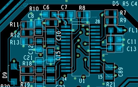
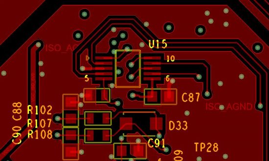
    I have attached the snapshots of board file both top & bottom layers. Also, I have attached the corresponding schematics so that you can decide on the components in the board file snaps based on the schematic reference designators.RTD trace length in our board is around 2.5 inches & we have maintained 2W separation from all other traces.

    0434.RTD_Schematics.pdf

    Also, we had a detailed analysis of changes in resistance values over the operating temperature range. We varied the input resistance from 10 Ohm to 4000 Ohm & measured the resistance after 5C variation in temperature. Please find the attached file for details.

    1323.RTD_Resistance_Measurement.xls

    At very low resistances (below 300 Ohms) the resistance to temperature curve is not linear but at higher resistances we observe that the as the temperature increases resistance also increases linearly. 

    Do you think this behavior will be similar on all the boards? Can we use this linearity to compensate for the error due to temperature variations.

    Please suggest.

    Thanks,

    Suresha N S
  • Suresha,


    I want to review some of the things that we've tried and see what else may be left.

    First as a review, I suggested removing the input filtering because I thought that the input resistors might react with the IDAC currents (this includes the resistor mismatch and their drift). This would remove R18, R19, R108, R107, R12, and R13. It's less likely R12 and R13 would make a difference because they are going into the reference.

    Another thing to try would be the removal of the AVDD filter. I thought that the added inductance would have added extra noise or caused some timing/sampling errors because the supply voltage may spike because of the digital currents.

    I also suggested that you remove the ADG704 because of any leakage current that it might bring to the measurement path. I would also note that the on-resistance might be a factor too. Since it's in the current path, it becomes part of the measurement. Note - in this measurement the O resistance and the P resistance are close to the same (but there is mismatch), but the N resistance is not the same. If you are still using the analog switch, go though the analysis again just to make sure.

    I originally asked about the RTD connections, but I didn't elaborate earlier. The way that you have this three wire RTD connected is not a typical hook up. Usually you connect the single wire to the positive terminal and one of the double wires to the negative terminal. To make the measurement, you drive the current throught the positive terminal and then the same current to the negative terminal. With this method you subtract out the resistances of the positive and negative wire connections. The third wire is used to shunt the current to a reference resistor and it's resistance never needs to be consider. If you can, set this up to run your system this way. I would have thought this would have been the best, most accurate solution.

    Let me know that you checked each of these points. I want to make sure we don't miss anything.

    Going forward, there are few other things to consider. First, are D9 and D33 in your circuit? Their leakage could contribute a certain amount of error. These diodes enough leakage to disrupt the measurement.

    Are these boards that you've built yourself? Have they been cleaned? The flux on the board from the soldering process should be cleaned off. The flux itself can have a resistance that can cause a leakage in either the RTD or reference path. It may not be a lot, but it is certainly enough to cause a noticeable error.

    You might be having problems with the switching of the IDACs. I would be more worried about this if you had larger input capacitors. If you select one RTD, made a measurement, then selected the other RTD and made a measurement, you need to make sure that there is time for the both the RTD and the reference to settle. By switching the IDAC, you can cause the current to momentarily go away (as the IDAC switched sources) and there needs to be time for the current to turn back on and settle to final value. You could add more time between samples to check this problem out.

    In reviewing your data, it looks as if the error is higher than I had originally thought. Just looking at the input resistance of 4kOhm, the measured value is 4093.662, which is an error of over 2%. On top of that you have an added drift of another 2% going from 10C to 60C. Do you know what the original source of the 2% error is?

    I took your data and checked to see if the error is linear with measurement and temperature. Going from 1kOhm to 4kOhm measurements, I calculated that the error isn't perfectly linear. I get about 3 ohms of nonlinearity at 10C going to about 5 Ohms at 60C (I decided to eliminate the lower values because they are smaller and would have more noise).


    If you take a single resistance value (as an example 4k) and look at the linearity of the measurement with temperature, going from 10C to 60C, the result is also not linear. I get between 7 and 8 Ohms of non-linearity in the measurement.

    Regardless, the absolute error and error drift are rather large. Look through my comments above. Make sure that you've gone through the items that we've talked about in previous posts, and check the material that we've talked about in this post. Respond back when you've been able to look through this.


    Joseph Wu

  • Here are some of the non-linearity plots, just in case you were curious. They are generated by removing the gain error and offset and plotting out the subtraction of the expected value from the measured value.


    It may not be that useful to you, but it does show that the error isn't necessarily linear to the temperature or the measurement. I would start by tracking down the large initial error that you have in the measurement.

    Joseph Wu

  • Suresha,


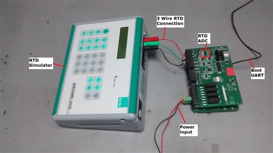
    While I'm thinking of it, can you please post a photo of your setup?

    Joseph Wu

  • Joseph,

    Please find the snapshot of our setup below.

    During our thermal chamber testing, using similar cables for connecting RTD simulator to our board, only difference being cables are much lengthier so that we can keep the RTD simulator outside the thermal chamber.

    We are analyzing your suggestions, I will post an update on the same by tomorrow.

    Thanks,

    Suresha N S

  • Hi Joseph,

    Sorry for the delay in response. 

    I have added all the discussion points in an excel sheet for easy tracking.

    0257.RTD_discussion.xls

    Please suggest on Item No 12,13 & 14 of the excel sheet. 

    Looking forward to your response.

    Thanks & Regards,

    Suresha N S

  • Hi Joseph,

    We have tried to measure the Vadc across RTD & Vref across Rref using Agilent 4401A precision multimeter.

    Please find the attached file for details. To measure the voltage using multimeter, we just kept the current flowing through the RTD always. Thus the conversion from ADC raw values to actual resistance is not enabled. 

    5126.Voltage_Measurement.xls

    As you can see, Vadc,Vref & Read value from RTD increases as the temperature increases. Although there is difference between actual read value from ADC to theoretical calculated value, we can see that the max to min variation is almost same in both the cases. We feel that the difference between actual & theoretical value can be removed using calibration at room temperature.

    Since there is variation in both Vadc & Vref, internal current source output must also be varying slightly. But the total variation is only 5.4mV whereas variation in Vref is 7mV. Our resistor is having a temperature coefficient of 10ppm/C & as per our calculation this shouldn't introduce such high errors. What is your opinion on this ?

    Also, can you please share your thoughts on the last query regarding RTD measurement architecture ?

    Thanks,

    Suresha N S


  • Suresha,


    First thanks, the data you took might be helpful in solving the problem. Let's start with the excel file. In the first column, you have temperature, which varies by 5.5C. It's not much, but it is enough to show some variation. Later, if you make future measurements, higher resolution might be better with the Vadc and Vref. I'd like it in the 6 digit mode, since 4 and 5 digits might not be enough. Another thing to keep in mind is that you want to set the multimeter in a high impedance mode. An input impedance of 10M, is just barely enough to affect the measurement.

    This is the important part: if you look at the ratio of Vadc to Vref, and you'll see that there is an drift. However, this drift matches the ADC measurement. This implies that the ADC is making correct measurements because the ADC matches the multimeter. Starting at the 26.75C measurement, you get a Vadc/Vref ratio of .937614, at 32.25C, the Vadc/Vref ratio is .938204. This is a change of 0.0629%. Now look at the ADC measurement. It goes from 7873216 to 7877907 in the same temperature range. This is the a change of 0.0596%. This is roughly the same change over the same temperature range - it's an error of only about 6ppm/C. It looks like the ADC is measuring correctly, and there is some error in the resistor/RTD setup, not in the ADC.

    Let's look at what the measurements may mean, starting with the reference voltage, and then going to the ADC input measurement.

    In the third column is the reference voltage measurement. This should be 4.3k (0.05% acc, 10ppm drift). Starting with the 26.75C measurement, this 1.978V, with 4.3k gives a 460.0uA of current from the IDAC. The problem is that the accuracy of the IDAC should be +/-6% max and 1% typ. In your case, you're already at -8% low. Is it possible that you have some other leakage path for current going to the resistor? Assuming that the resistor is really 4.3k, the result at 32.25C shows 1.971V. At that point the current would be 458.3uA. Assuming that that current is accurate, then the drift is (460-458.3)*(1e6)/(460*5.5) = -672ppm/C. This would be much larger than the typical 100ppm/C. While there is some drift associated with the IDAC, this is far larger than expected. Again, I would suspect there is some other leakage path that may be steering current away from the reference resistor. One thing you could do is physically short the IDAC output to ground through an ammeter, just to make sure the original IDAC current isn't closer to 500uA.

    Looking at the the ADC measurement, Is this resistance 4.030k? If that is the case, then I get 460.20uA at 26.75C. Again, the current is off from the expected value. However, you can try to relate the current through the input measurement and the reference resistance. If resistance is 4030 Ohms, the current through the input resistance the reference resistance are off but it's very small (< 0.5uA).

    Since the error is very small, it could be several things, however, the error seems to get more positive as the temperature rises. It looks like there's extra parasitic resistance with a positive temperature coefficient for the Vadc measurement, or there is a higher leakage away from the Vref resistor as the temperature gets higher.

    One thing to look at is the layout. I just noticed the size of the traces going to the inputs. Trace back the inputs to AIN0/AIN1. If you follow traces through R18 and R19 you'll see that most of these traces are 3 mils wide (thats a guess, it's hard to tell on a picture). I'm not sure about your copper weight, but I'm sure that this has a moderate resistance as a PCB trace. Also, how do you short R18 and R19? If you are using a "0 Ohm" resistor, it's probably has enough resistance to disrupt your measurement. The trace resistance is a problem if it is this narrow all the way to the RTD connector. You could try to make a guess about how much trace resistance is, but I can't see the entire layout. Also note that with such small traces, the tolerance error becomes a large part (as an example, what is the resistance for a 3 mil trace if the error is +/-1mil?).

    The way most people measure a three wire RTD, they will drive the IDAC through AIN0, then through AIN1, and then subtract, using the third line as the return path for the reference. However, in your case, you use the third wire as one of the IDAC drives, then use AIN0 as the second drive, using AIN1 as the return for the reference. However, trace paths for IDAC OUT and AIN0 may not be similar (this isn't shown in the layout pictures). Again, you can try to calculate out with some PCB trace resistance calculator what the resistance is.

    As for the last question about the RTD measurement architecture, Are you asking about the 2-wire RTD measurement? If you make a 2-wire RTD measurement, you still need to connect the RTD negative input to the reference on your own. It's the least accurate measurement, since you can't remove the parasitic line resistance.

    Joseph Wu

  • Hi Joseph,

    As you have pointed out correctly, we were measuring the voltage using multimeter in 10MΩ input impedance mode. Because of this we were observing a dip/increase in the ADC reading whenever we connect/disconnect multimeter. Thus we thought that analyzing further with the old data is not correct.

    We increased the input impedance to 10GΩ & took the readings once again. With this input impedance we didn’t observe any variation in the ADC reading when we connect/disconnect the multimeter. Along with this we have also changed the multimeter settings to get readings in 6 digit mode. We found that the Vadc/Vref ratio is matching with the ADC readings with this data also.

    As per your suggestion, we connected the IOUT from ADC directly to ammeter for IDAC accuracy. We also added different series resistors (in the range of 100Ω to 8.3KΩ , which covers the actual RTD + Rref range) to check out the effect of load resistance on the IDAC output current. The current was constant with different loads. Also, to find out the IDAC drift during temperature variation, we have kept the series resistor to be constant at 8.3KΩ & measured the current at different temperatures. We have selected 8.3KΩ for this analysis since 8.3KΩ corresponds to our actual load when we connect 4KΩ RTD with reference resistor being 4.3KΩ. Here also, we found that there is very minimal drift at the output of the IDAC.

    Thus we concluded that, as you suggested, the issue is with the ADC input rather than IDAC output or the ADC measurement. 

    With this in mind, we thought about the components in parallel to RTD input, which may cause the variation in input. Actually, we had a ESD protection diode at the RTD input pins. We removed these diodes & the IDAC output was increased to 497uA & there were no variations in the RTD measurement readings. You had already suggested that the zener diodes D9 & D33 present in the schematics may cause the issue. But these were DNI’s & the actual ESD protection diodes were present on the other page of schematics. I should have thought about these diodes much earlier, which could have saved a lot of time. 

    We have put the board into the thermal chamber after removing the protection diodes. We find that the accuracy over the operating temperature range is very good. Please find the attached excel sheet with our measurement results over the operating temperature range.

    6505.Resistance_Measurement.xls

    We need to protect our board from ESD (IEC61000-4-2 , Level 2) , EFT (IEC61000-4-4, level 2) & Surge (IEC61000-4-5, level 3). Thus we had included the protection diode 1KSMB6.8CA on the RTD input pins. Have you used any such protection diodes with ADS1248 ? If so, can you please suggest for an alternate diode which we can use in our case.

    Just to answer your queries on last post, we have routed all the RTD traces with 6mils trace width & 12 mils spacing.  Also, I had a look on TIPD120 circuitry during design, but changed our architecture to accommodate our requirement of supporting both 2-wire & 3-wire RTD connections on the same terminal.

    I would like to thank you for your support during our RTD debugging.I learned a lot from these discussions.

    Regards,

    Suresha N S

  • Suresha,

    I'm glad you're on the right track. This was a tough problem to debug because the effect is small and it requires a lot of data taking to track down the real problem. It seems that you now have it under control.

    As for the TVS, I don't have any great recommendations because I've never used any. I looked a the Littelfuse TVS that you mentioned and I'm not sure it will work for you. I've used other Littelfuse TVS diodes for power applications, and really like them, but this application requires extremely low leakage and this diode specs a max of 1uA. You can try it, but I think you want to be a couple order of magnitudes lower in leakage.

    A quick look through the TI portfolio shows that the lowest leakage device would be a quad channel TPD4E110 (at < 1nA) or a TPDxE05U06 (at < 10nA). I've never used either and I'm not sure if they fit your ESD and surge requirements.

    One last note on the input traces. If you can go larger than 6 mil as a trace width, I would. It depends on the copper weight that you use on your PCB, but I'd really try to reduce the trace resistance so that I don't have to worry about it.

    Again, I'm glad you were able to get your system debugged. If you have any more questions, feel free to post again. I'd start a new thread - it's getting hard to search through it.

    joe wu

  • Hi Suresha and TI team,

    Have you got an answer regarding the assumption described in the previous post? Are the variations described by Suresha due to ambient temperature variation impacting ADC ADS1248?

    Thank you in advance for your reply.

    Fabrice
  • Fabrice,


    It's been a long time since I've reviewed this post and I'll admit I've forgotten a lot of it. However, I think there were a combination of issues with this and one of the important ones was some input protection diodes that caused some leakage that reacted with the measurement.

    There's quite a bit to read through. There were 24 posts of back and forth debugging. Hopefully you didn't just see the one page (of three) that were in this post. Perhaps Suresha could comment further?


    Joseph Wu
  • Hi Fabrice,

    As Joseph suggested, this issue was caused by the ESD protection diodes we had in the RTD input. 
    There was a significant leakage current flowing through the diodes which used to vary with respect to the temperature.
    Thus we were observing the variation in measured RTD resistance.

    After we removed the ESD diodes, there was no issues with accuracy & drifts related to temperature variations were within the specified limits mentioned in the ADS1248 datasheet.

    Hope this helps.

    Thanks,
    Suresha

  • Hi Suresha and Joseph,

    Thanks for your replies. I have now also read the page "RTD Measurement using ADS1248 : Protection circuitry on input pins" and it helped a lot.

    Is the ADS1248 TI best ADC at the moment to read accurately and with higest resolution RTD temperature or even thermocouple?

    Thanks,

    Fabrice
  • Hi Fabrice,

    we have multiple ADCs that are perfectly suited for RTD and thermocouple measurements. ADS1248 is probably the most popular right now. If you want even higher accuracy then you might want to look at our new ADS1262. In case you want something simpler than ADS1248, then ADS1220 is a very good choice.

    Regards,

  • Hi Joachim,

    Thanks for your answer. This is informative.

    Best regards,

    Fabrice