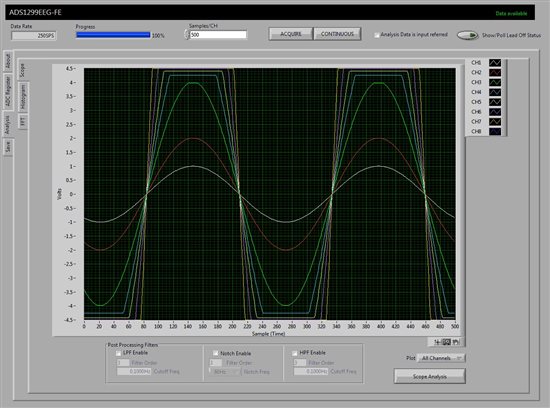
I am using the ADS1299 in a new design and ran into some behavior while I was debugging that I am unable to explain.
The output range of the internal amplifiers seems to vary based on the gain settings. AVdd for the converter is +5V. I have a single ended input signal on Vin+ centered around 2.5V and Vin- is 2.5V. Vref is the internal 4.5V. With a gain of 1, the A/D converter is measuring +2.5 to -2.5, which is what I would expect. With a gain of 2, the A/D converter measurement ranges from +3.3 to -3.3, outside of which it clips. The clipping is not a hard digital value. There is some variation, including somewhat of an inversion of the sine wave tip, increasing as the overdriven input increases. As gain increases, the ADC range increases, but it isnt until a gain of 12 that the full +/- 4.5V range can be seen.
The values for each of the gain settings are as follows
Gain Vadc
1 +/-2.5
2 +/-3.3
4 +/-3.9
6 +/-4.25
8 +/-4.4
12 +/-4.5
24 +/-4.5
Vadc is the output voltage from the converter, not compensated for gain setting.
I initially found this behavior debugging my custom design, but I tested it with the ADS1299EEG-FE development board and found the same thing.
I wasn't able to find anything in the data sheet to explain what is going on. The amplifiers are described as differential input, differential output amplifiers that drive to within 0.2 of the power supply rails, so the output should be +/-4.6V (clipped at +/-4.5V by the ADC) regardless of gain setting.
The part is being used in an EEG application, so signal levels will not ever reach these amplitiudes, but DC offsets can be large and I need to understand what the part limits are so I can properly specify the input range of our device.
Tom


