This thread has been locked.

If you have a related question, please click the "Ask a related question" button in the top right corner. The newly created question will be automatically linked to this question.

DAC121C085 - Analog output timing

Guru 19775 points
Other Parts Discussed in Thread: DAC121C085

Hi Team,

I would like to ask you about DAC121C085 analog signal output timing.At which timing does the device outputs the analog data which is converted from the input digital data ? There were no timing chart in the datasheet which shows SCL, SDA,and VOUT.

In our customer evaluation, VOUT starts to rise and output the analog data right after it receives the data, before the I2C NACK and STOP bits.

Is this the normal operation for DAC121C085 ?

Best Regards,
Kawai

DAC121C085 I2C and VOUT waveform.pdf
  • Hi Kawai,

    Your customers observations are in line with the device definition.

    The DAC input register is updated on the rising edge of SCL that would clock in the ACK for the second data byte - the DAC output will immediately start responding to the new value in its input register.

    NOTE: If the STOP occurs before this edge, the data received will be discarded.

    Sincerely,

    tom

  • Hi Tom-san,

    Thank you very much for your support. 

    Please let me confirm again. I understand your explanation if channel4 was the waveform of VOUT pin, however, the waveform of VOUT pin is channel1(blue) in the figure. If you look at the rising timing of channle1, it rises immediately after bit0 of the second data byte, before the rising edge of SCL for ACK. This was my question if the device is operating normally or not.

    Best Regards,
    Kawai


  • Hi Kawai,

    Indeed, I was looking at the wrong trace...

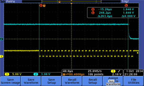
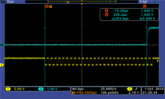
    Anyway, I just picked up a random DAC121C085 coducted the same test as you did. I have attached the scope images. Bottom line: the VOUT is updated on the falling edge of the BIT0 clock of the second data byte. It is consistent with your observations. I did this measurement for both falling and rising VOUT...

    BLUE -> VOUT; YELLOW-> SCL

    So, this appears to be the normal operation of this device - not quite the way I described it in my previous post.

  • Hi Tom-san,

    Thanks for the data.

    I understood that this is the normal operation for this device.

    I greatly appreciate for your support!!

    Best Regards,

    Kawai