This thread has been locked.

If you have a related question, please click the "Ask a related question" button in the top right corner. The newly created question will be automatically linked to this question.

ads1278 power down problem

Other Parts Discussed in Thread: MSP430F5529, LM317, THS4521, ADS1278

Hi TI Forum,

I am using AD1278EVM REV E for my thesis and I use MSP430F5529LP to read data from ADC by SPI. The settings are as following:

S2 on ADS1278EVM: High resolution, TDM Fixed,

CLK: 8MHz from SMCLK (pin2.2) of MSP430F5529,

SCLK: 8MHZ from SPI (pin2.7) of MSP430F5529,

I give the supplise from MSP430F5529LP (+5V and +3.3V and generate 1.8V using LM317 from +5V).

I connect the pins on ADS1278EVM and MSP430F5529LP by cables as in Figure (1)

I am using MSP430F5529 integrated USB module to send data to computer and read data using MATLAB.

                                                                                  Figure (1)

I have two problems:

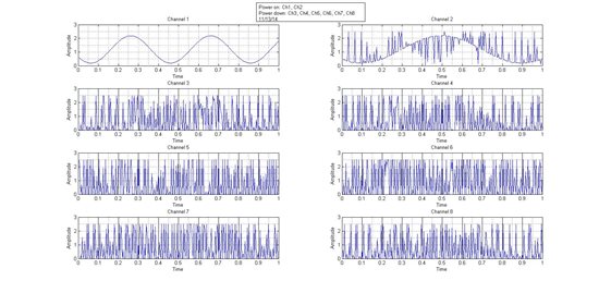
1.  I try to read data from multiple channels . I apply 1V sin waves  to channel 1 and channel 2 powering down all the other channels  by S1. I receive the wrong output as in Figure (2). I expect channels 3 to 8 to be zero but they are not. In addition channel 2 is very noisy that I cannot apply signals with smaller amplitude.

                                                                                                                   Figure (2)

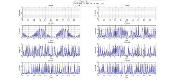
Then I apply the same signals to channels 3 and 4 powering down the remaining by S1 (Figure 3). This time channels 1 and 2 are ok giving right output (zero) but channels 5 to 8 behave the same way. In addition data from channels 3 and 4 are very noisy that in channel 3 I can only see envelope of the input signal and in channel 4 it is barely recognizable. 

                                                                                                                 Figure (3)

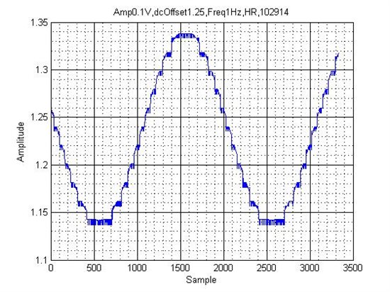
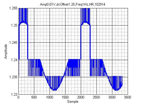
2. My second problem is with small amplitudes and lower frequencies. I need this device to detect signal about 1mVp-p and frequency of 1Hz. As I decrease amplitude and frequency I come up with the problem in Figure (4) and Figure (5). Inputs are 100mV, 1Hz and 10mV, 1Hz respectively. 


Here is the section of the code I am using to read data through SPI:

    UCA0CTL1 |= UCSSEL_2 + UCSWRST;   		   
   UCA0CTL0 |= UCCKPL + UCMSB + UCMST + UCSYNC ;  
   UCA0BR0 |= 1;                       
   UCA0BR1 &= 0;
   UCA0MCTL = 0;                         
   UCA0CTL1 &= ~UCSWRST;                       


    while(1)
    {
		for (counter = 0; counter < 24; counter++)
		{
			UCA0TXBUF = TX_Data;
			while (!(UCA0IFG && UCRXIFG));		
			DataBuffer[counter] = UCA0RXBUF;
		}
     }


Thanks

Reza

11/13/14

  • Hi Reza,

    Thanks for your questions! Have you managed to get this working yet?

    There may be a few things going on here. First, I have some suggestions from the analog input side:

    • Figure 1 shows that you are attaching the inputs from the signal generator to Channels 3 and 4, not 1 and 2.
    • Also, since the ADS1278 in an unbuffered ADC, you really should take advantage of the on-board THS4521 differential amplifiers. They will help drive the input cap and set the input common-mode to mid-supply.

    What settings are you using for Mode [1:0], CLKDIV, and FORMAT [2:0]? Can you send us a capture from a logic analyzer so that we can verify your SPI timings?

    Best Regards,

  • Hi Ryan, 

    Thanks for your fast reply. I have tested several channels by applying inputs. On figure above, you are right I share the figure in which I tested channel 3, and 4. But I am using just channel 1 to get the correct response.  As you suggested, in the my new results I am using on-board THS4521 by S8 and removing JP3 (PD_Buffer). Unfortunately I didn't have access to logic analyzer now, and I use oscilloscope to track the signals. In the following are the figures shows 1mV, 10mV, and 1V, input signal with frequencies between 1Hz, and 10Hz. The point is that as the amplitude and frequency of signals grows I have less and less problem.

    ADS1278EVM configuration: MODE: 01 (High Resolution), CLKDIV =1, FORMAT: 001 (Fixed-TDM), adjusted by S2 on ADS1278EVM,

    Except channel 1 remaining channels are powered down by S1 on ADS1278EVM. 

    I feed CLK=SCLK=4MHz from MSP430F5529LP and MSP430F5529 works with MCLK = 8MHZ.  

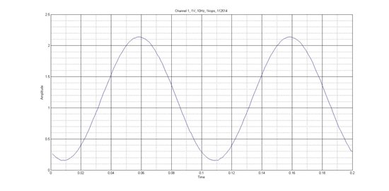
    Figure 1: There is no problem

    1V, 10Hz, 1ksps,  

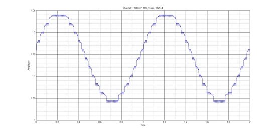
    Figure 2: There is a problem. The steps all have amplitude of 10mV, and are not random. 

    100mV, 1Hz, 1ksps, 

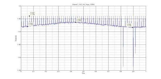
    Figure 3: Exactly 10mV spike, again not random.

    10mV, 1Hz, 1ksps

    Figure 4: The problem is disappeared.  

    1mV, 1Hz, 1ksps

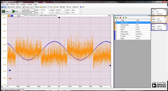
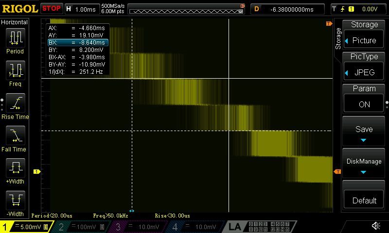
    I try to find logic analyzer and send you the SPI analysis. As you see the spikes are 10mV and not random. In the figure below I send you the capture of input to AINP1 (blue), and AINN1 (orange),  AINN1 is connected to ground. As you see I get the projection of the AINP1 on the AINN1. May it be a problem since AGND and DGND are connected together? By the way I measured AINN1 (is grounded) with respect to power supply ground.


    And one question? As I understand SCLK in ADS1278 is a clock data output rate, and CLK is for modulator. Is it right?

    And finally is it possible because of fail in ADS1278EVM? (I have just one)

    If you can give me an e-mail,  I can share my codes with you.

    Thanks

    Reza

    11/25/14 


  • Hello Reza,

    In addition to removing the jumper on JP3, the switch S8, should be moved to the right position to select the BUFR option; otherwise, the inputs from J3 are routed directly to the ADS1278. Did you already do this?

    I see that there is some confusion among the different clocks and data rates used in the ADS1278. Allow me to clarify:

    • The master CLK of 4MHz is the main clock frequency for the ADS1278. The frequency at which the modulator samples the inputs (known as fMOD) is derived from CLK and it depends on the Mode and CLKDIV settings. The table below combines the information from the datasheet tables 6 and 8.
    • The output data rate is calculated by fMOD / OSR, where OSR is the over-sampling ratio. In High-Resolution Mode, the OSR is 128.
    • Mode [1:0]

      Mode Selection

      Max fCLK

      (MHz)

      CLKDIV

      fCLK/fDATA

      fMOD

      OSR

      00

      High-Speed

      37

      1

      256

      fCLK/4

      64

      01

      High-Resolution

      27

      1

      512

      fCLK/4

      128

      10

      Low-Power


      27

      13.5

      1

      0

      512

      256

      fCLK/8

      fCLK/4

      64

      64

      11

      Low-Speed

      27

      5.4

      1

      0

      2,560

      512

      fCLK/40

      fCLK/8

      64

      64


    • The SCLK is the SPI clock frequency used to shift data out of the ADS1278. This clock must be fast enough to read out all of the data before the next conversion is finished.

    Does this make more sense? Have you been following the timing specifications for SPI?

    Best Regards,

  • Thanks Ryan,

    I was confused with data output rate and and the time (SCLK) to read data. I thought that I can read each bit in (fDATA /512 ) but it was wrong. Data output rate determines DRDY but each bit is sent out by SCLK,  so, I have to read much faster than what I was doing previously. But how about the SCLK = CLK/2 or SCLK = CLK/4? Do we lose bit or bit when SCLK is divided? I think there must be a lower limit for SCLK because all the bit have to be sent aout and read before the next DRDY comes. Is it right? 

    And I looked at my input signal to the ADS1278EVM in details in oscilloscope. The figure below shows that it has step like shape which may cause the problem I am facing but I am not sure.  

    I should modify my code to read the data with respect to SCLK because certainly I am losing some bits. 

    Thanks for fast reply

    Reza

    12/08/14

  • Hi Reza,

    It looks like you have figured it out!

    The minimum SCLK that you can use will be determined by the number of channels that you read and the output data rate you set using the table above. For example, if the device is configured to produce an output data rate of 100kSPS, and you wish to read 4 channels (24 bits each), your minimum SCLK rate would be 100E3 x 4ch x 24 bits = 9.6MHz.

    Best Regards,