This thread has been locked.

If you have a related question, please click the "Ask a related question" button in the top right corner. The newly created question will be automatically linked to this question.

RTI noise, Test signal and normal mode offset in ADS1294 ?

Other Parts Discussed in Thread: ADS1294

Hi .

I design my board for ADS1294. wen I want to use first time , I want to check it;s input reffered noise and test signal and normal input. this are my Data that sent to ADS1294 :

CONFIG1 : 0x05     // Fmod : 500 SPS  ,   Low power mode

CONFIG2 : 0x10     //  Internal test signal enable  with default amplitude and frequency

CONFIG3 : 0xE0        // Enable internal reference voltage with : Vref = 4 volt (AVDD = 2.5 , AVSS = -2-5) ;

I configure Channel 1 with  0x61    // Gain = 12 ; Input shorted .

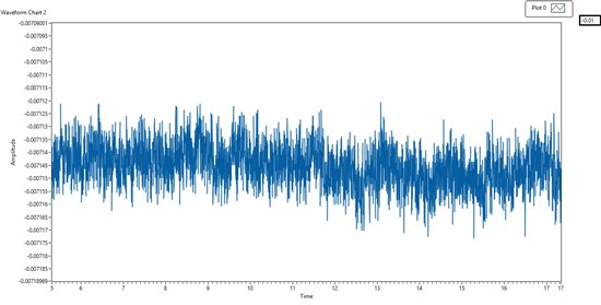
below is my signal in PC :

1. as you can see in the graph, RTI noise is approximately 30uV P-P , but in datasheet it is about 3.2 uV P-P. in your opinion this difference come from where ? if we raise the PGA gain RTI noise (or other noise that are same) must be decrease but in this case it doesn't work !!

2. I changed channel situation with this configuration :

CH1SET = 0x60       //      Normal input  ,   Gain is 12

CH2SET = 0x81       //       Channel Power down

CH3SET = 0x65       //      Test Input      ,     Gain is 12

CH4SET = 0x11      //        Short input    ,      Gain is 1

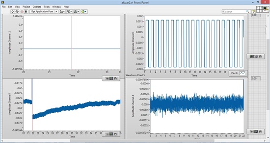
this is my outputs :

plot below,right is channel 4 with input shorted noise with approximately 30uV P-P. this time gain is 1 but noise level doesn't change rather than G = 12 . why ?

3. plot up right is Chanel 3 with internal test signal with G=12. internal test signal is default f=1Hz and amp=4/2.4 mv . but it is not equal to my plot amplitude ?

4. below left plot is Channel 1 with normal input and G=12 . input electrode are free and doesn't connect to any signal. just input low pass filter but it is approximately -0.65 V DC and it fluctuate and rise up. where come this DC offset ?

I don't place R21 yet.

forgive me because of my weak grammar and I appresiate your answers.

Thanks.

  • Hi Mohsen,

    Sorry for the delay in my reply.

    1. The first data plot does not appear to be input-referred. I estimated the peak-peak noise to be about 38uV from this graph. 38uV / 12 = 3.167uVpp. Make sure that you are dividing the result by the PGA gain in your calculation.
    2. For Gain = 1, the peak-peak noise should be closer to 17uVpp. I believe the data in the Noise Measurement tables is +/- 1-sigma of the noise distribution recorded for each setting. How are you measuring the peak-peak noise? Are you taking the global max/min? Excluding some of the obvious outliers, the peak-peak noise looks closer to ~20uVpp.
    3. Test Signal = (4 / 2.4) mV = 1.67mV amplitude, 3.33mVpp. Please check VREFP and VREFN. For a 4V reference, VREFN  should be tied to AVSS = -2.5V and VREFP should be 1.5V.
    4. Do you have lead-off enabled on Channel 1? The internal pull-up resistors or lead-off current sources may be charging/discharging your input RC filter when no inputs are connected. Also, the capacitors C45 and C46 must be placed following the resistors in the input signal path to get the RC filter response.

    Best Regards,

  • Thanks for your reply.

    1,2 : as I understand from your reply, input shorted noise in every Gain must be divided to Gain and answer is our input shorted noise of ADS1294. with considering your reply and look to datasheet, input shorted noise same and I can say ADS1294 run correct. if we use normal mode on channel maximum noise from ADS1294 on input signal is this value (input shorted noise) ?

    3. I test it and say VREFP voltage to you. but I am sure that VREFN is connected to AVSS = -2.5 ; in below you can see schematic of that part with 10uF tantalum capacitor polarity.

    4. I only program mentioned register and other register is in default value. how I can disable lead-off on each channel ? if electrodes connect to input of each channel, this offset can remove ? for eliminate this offset what I can do ?

    Thanks for your reply.

  • Hi Mohsen,

    The noise that you measure with an internal input short is the noise contributed by the internal circuit components in the ADS1294 itself (PGA, ADC, etc.). Once the channels are operating in the Normal Input configuration, external noise from other on-board components and the environment will introduce additional noise in your results.

    To test the offset of each channel, you should take a measurement with the inputs shorted. The differential offset will be the average value of the output. For example, Figure 17 of the User's Guide shows the different offsets seen from all 8 channels with the inputs shorted. The results you observed on Channel 1 will change once you drive a signal into that channel and the inputs are no longer floating.

    Best Regards,

  • Hi Ryan, 

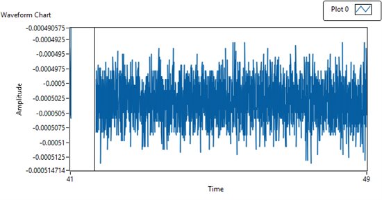
    I measure VREFP and VREFN voltage and they are +1.502 , -2.490 Volt. I program ADC1294 again and channel 1 to shorted input  and G=1, below is answer : 

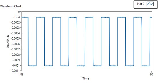
    and after that I programmed it to Test input (with default values) and G=1, here is the plot :

    1. in both plot DC offset on channel is very low and we can say it is approximately 0 , but this channel on the my first post DC offset for this channel is about -0.7 volt in normal mode. where come this issue ?

    2. why test signal amplitude still is wrong value with regard to data sheet ? some times amplitude of test signal (with default register value and G=1) is big as 0.25 v, and it is strange for me !

    3. I have another question from you. in datasheet and absolute maximum of voltages datasheet said that INN and INP input voltage must be between AVSS-0.3 to AVDD+0.3 , if input of one channel crossed this value (e.g. INN=0, INP = 3.3 v) , then this channel will be damaged or Whole ADC1294 ?

    Thanks for your reply.

  • Hi Mohsen,

    Thank you for verifying the reference voltage. Those are the correct values that I expected for VREFP and VREFN.

    mohsen hamun said:
    1. in both plot DC offset on channel is very low and we can say it is approximately 0 , but this channel on the my first post DC offset for this channel is about -0.7 volt in normal mode. where come this issue ?

    As I said earlier, I do not believe that the data you showed in that image was truly input-referred. The peak-peak noise seemed to be close to datasheet specs when divided by Gain = 12. Similarly, -0.7V / 12 = 583uV, which is close to the 500uV typical datasheet spec for offset.

    mohsen hamun said:
    2. why test signal amplitude still is wrong value with regard to data sheet ? some times amplitude of test signal (with default register value and G=1) is big as 0.25 v, and it is strange for me !

    Can you try to use the 2.4V reference and see if the Test Signal amplitude changes to the correct value?

    mohsen hamun said:
    3. I have another question from you. in datasheet and absolute maximum of voltages datasheet said that INN and INP input voltage must be between AVSS-0.3 to AVDD+0.3 , if input of one channel crossed this value (e.g. INN=0, INP = 3.3 v) , then this channel will be damaged or Whole ADC1294 ?

    (1) Stresses above these ratings may cause permanent damage. Exposure to absolute maximum conditions for extended periods may degrade device reliability. These are stress ratings only, and functional operation of the device at these or any other conditions beyond those specified is not implied.

    I do not suggest that you try it.

    Best Regards,