This thread has been locked.

If you have a related question, please click the "Ask a related question" button in the top right corner. The newly created question will be automatically linked to this question.

ADS1282 1 Channel Results

Other Parts Discussed in Thread: REF5050, ADS1282, ADCPRO, DAC1282

Dear Christopher,

Since our last contact I have the opportunity to make some progress in my application.

I still have some open issues and I want to share my doubts and some conclusions as well.

Before show you some DC and AC Analysis for different tests I suppose it’s important to give you an overall of the input circuit diagram and pcb layout used in this first prototype.

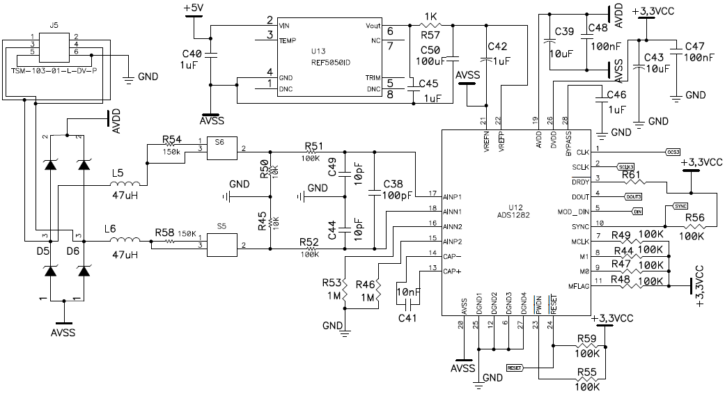
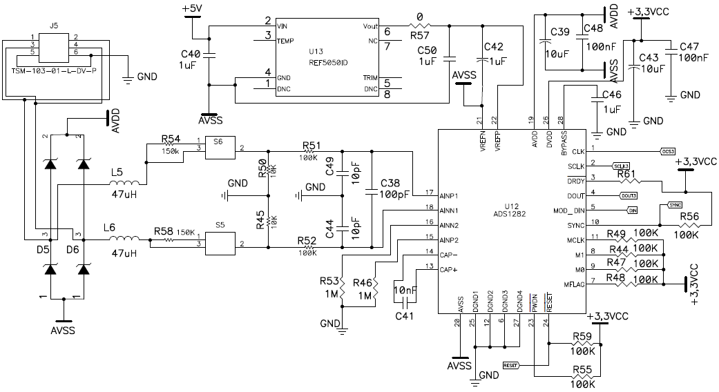
In the picture below you can see the electrical diagram of one channel (input circuit, AD converter, REF5050 …)

                                                               Picture 1 – Input 3 diagram

AVDD and AVSS are provided by TPS79225 (+2,5V) and TPS72325 (-2,5V), and a DC-DC converter (+-5V) is used to feed those regulators and other peripherals in the entire circuit.

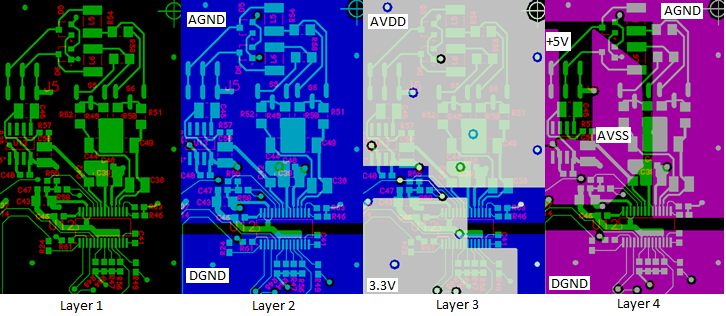
In the picture below you can see the pcb layout layer by layer for the input diagram (Picture 1). PS.: In the layout below please disconsider C45 from the pads connecting REF5050 Pin5 (TRIM) and AVSS, and instead this I installed a 1uF C45 0603 capacitor between REF5050 Pin6 (Vout) and AVSS like the input diagram (Picture 1). 

                                                               Picture 2 – Input 3 PCB Layout

Question 1:

Looking for the circuit diagram and pcb layout there’s something I could change to improve my circuit performance? I’ll show you some AC and DC analysis latter.

Question 2:

In our last contact I told you I intended to use the network (R54, R50, R54, R58) as an attenuator with a factor of 1/16 because the sensor output range (+-20V) can decrease the signal amplitude to +-1.25V to match the ADS1282 PGA input operating range (AVSS + 0.7; AVDD – 1.25). Is this range true or I can use a signal range from -2.5V to +2.5V? The reason I want know is because my Vref = 5V (Vrefp= +2,5; Vrefn = -2,5), so limiting my input signal from -1.25 to +1.25, I’ll lost resolution from my ADC. In this case should I use a PGA multiply factor 2 to match the desired ADC input range (+-2.5V), I think if I use a factor 2 for 250SPS I’ll get almost the same performance as I use a factor 1?

Question 3:

Should I use the RC filter (R57, C50) after the output of REF5050? The reason is because this resistor in series with the ADS1282 Vref input impedance cause voltage attenuation, measuring with a true RMS multimeter I found +2.450V between Vrefp pin and GND instead of +2,50V from the REF5050 Vout pin.

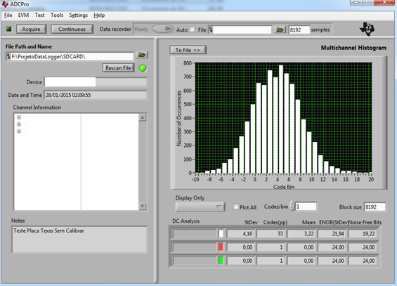
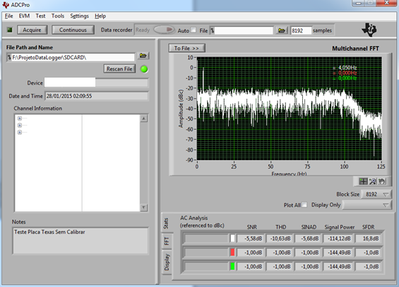
Questions regarding circuit evaluation using ADCPro (ALL TESTS PERFORMED USING Vrefp = +2.5V, Vrefn = -2.5V, 250 SPS, HIGH-RESOLUTION, LINEAR-PHASE, SYNC + LPF filter, AINP1 & AINN1, PGA CHOPPING ENABLE, G = 1):

I used the AC and DC analysis from ADCPro software to evaluate my circuit and the first problem I found was to adapt the results in a spreadsheet file format that ADCPro could read and evaluate the results.

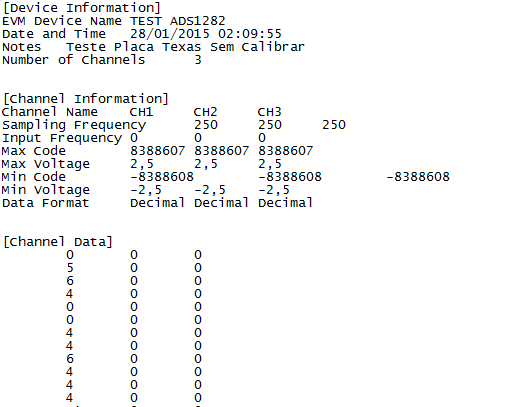
Unfortunaly during the first test I discovered ADCPro was not able to read 32bit integer values and interpret the results, so I decided to divide each sample by 256 to represent only 24bit integer values (Max Code 8388607, Min Code -8388608) as you can see in the picture below. Doing in this way ADCPro was able to evaluate the results.

Picture 3 – ADCPro file format

Question 4: Is there a way to allow "ADCPro File Reader", read and evaluate 32bit integer value samples?

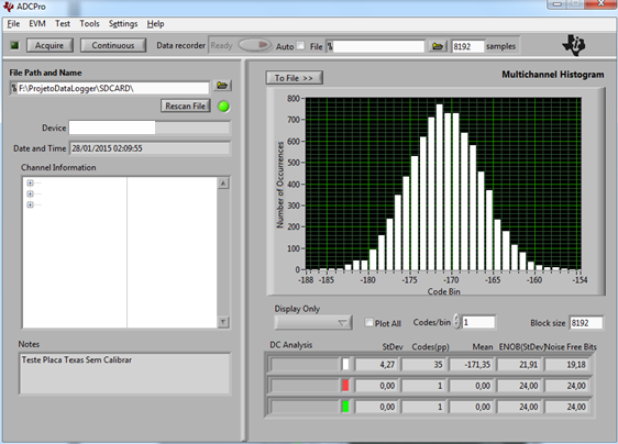
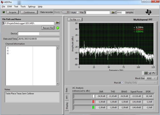
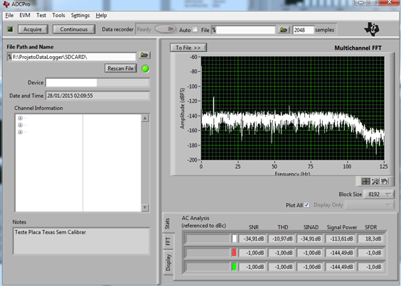
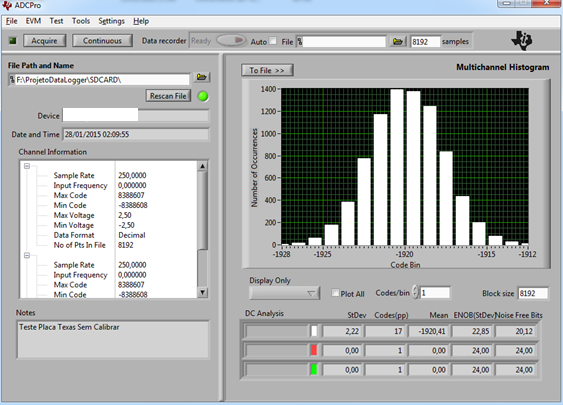
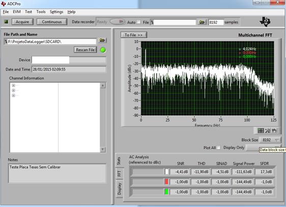
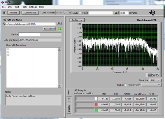
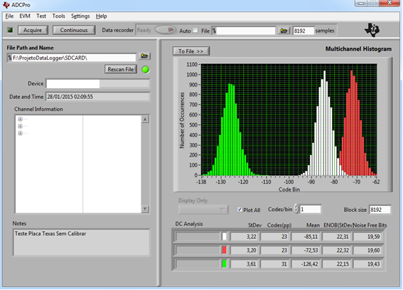
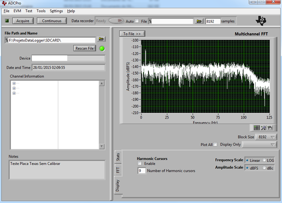
The first test I performed was without any calibration (Gain/Offset), no attenuation (R54, R58 bypassed by switches S5 and S6), shorted input Pins 1 and 3 of J5. In the next pictures you can see the AC and DC Analysis from the first test.

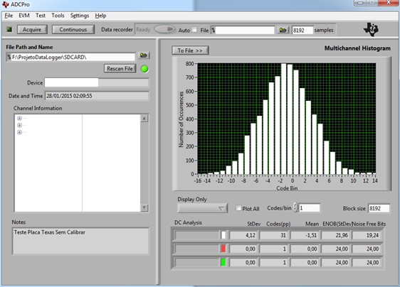
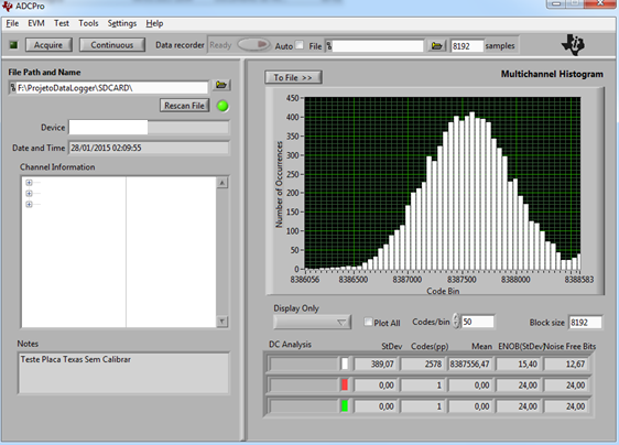
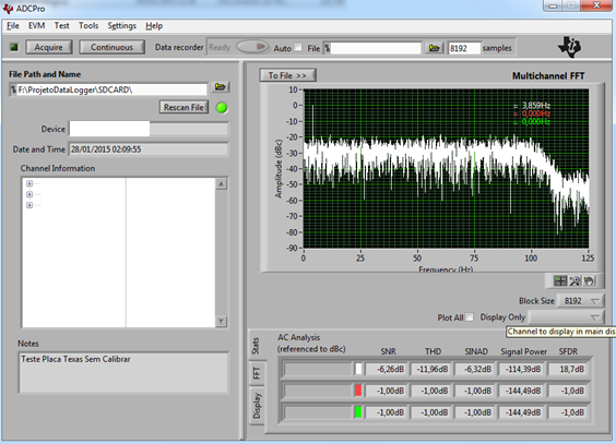
                                               Picture 4: DC Analysis 1st test

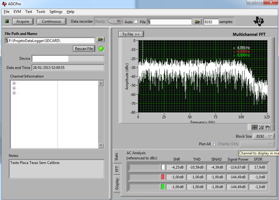
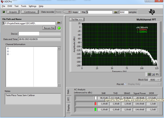
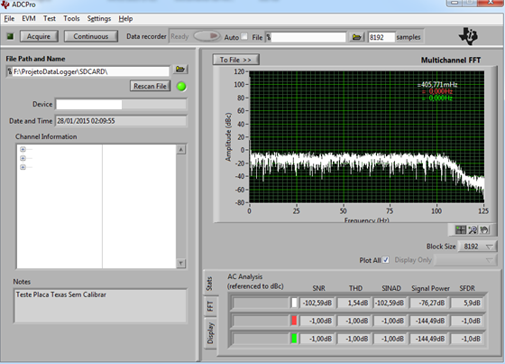
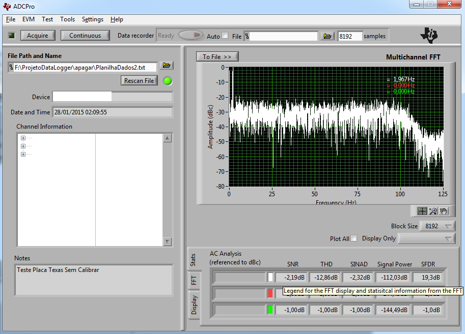
Picture 5: AC dBc Analysis 1st test

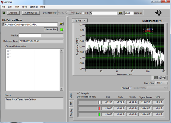
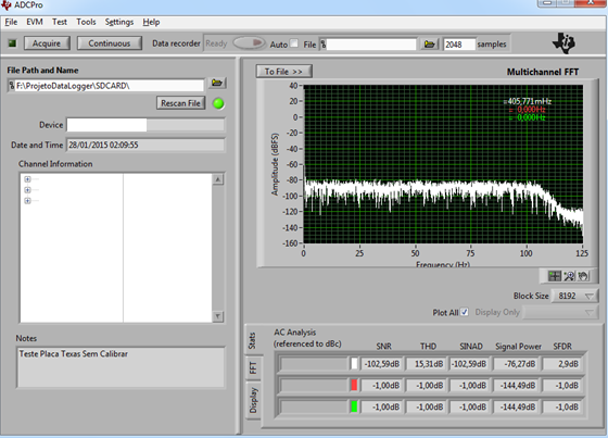
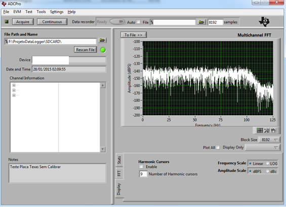
Picture 6: AC dBFS Analysis 1st test

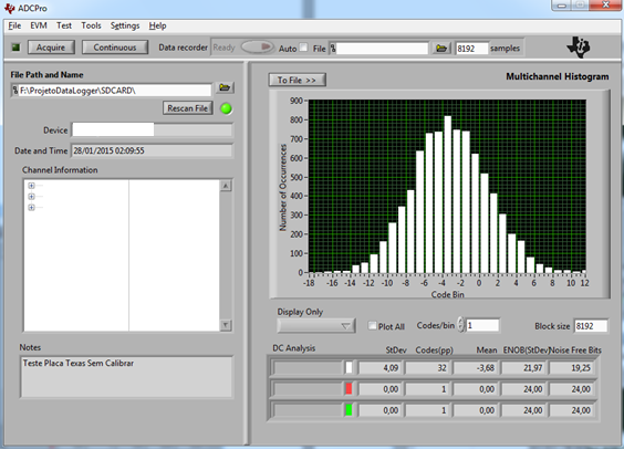
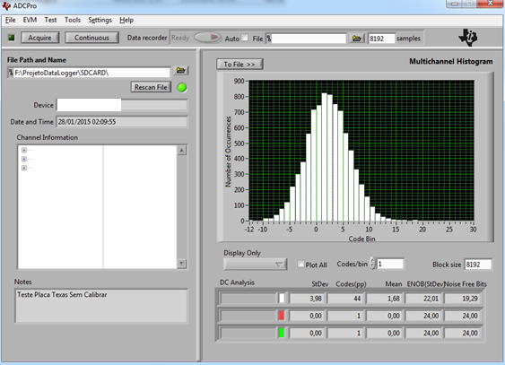
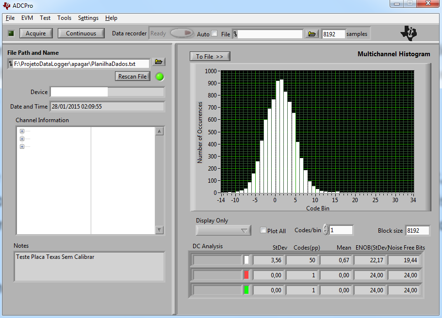
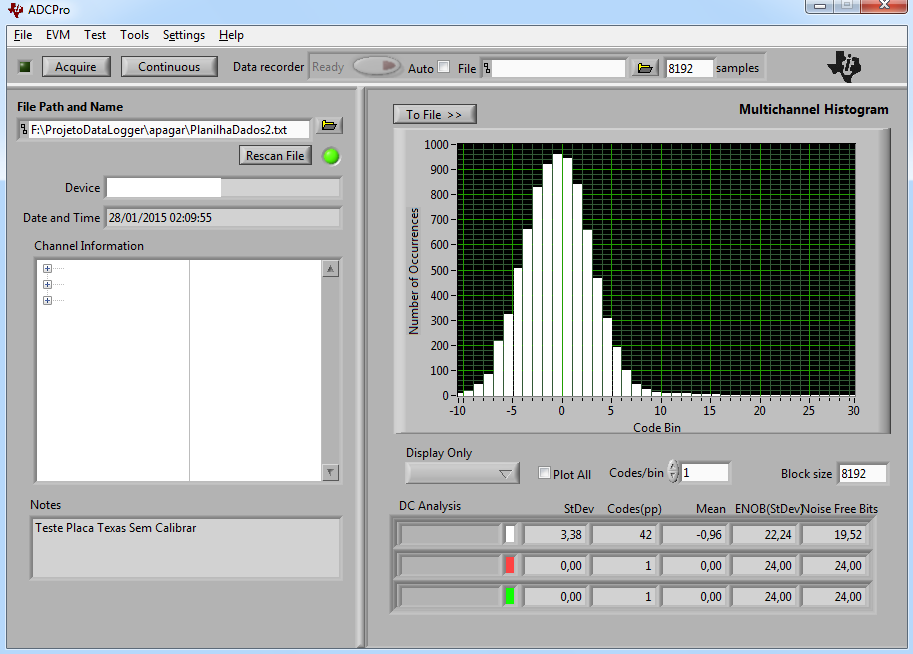
Question 5: Is there any possibility to improve the actual ENOB (21.91)? I did the same test with Texas ADS1282EVM board and reach the following results:

Picture 7: DC Analysis ADS1282EVM

Question 6: Could you help me to understand the results from the Picture 6? As I can see in the ADS1282 datasheet page 6, the SNR of ADS1282 for a shorted input and 1000SPS reach 124dB, the SNR result in Picture 6 was -34,91dB, probably the difference between the 0Hz (DC) signal amplitude and the 8.338Hz component.

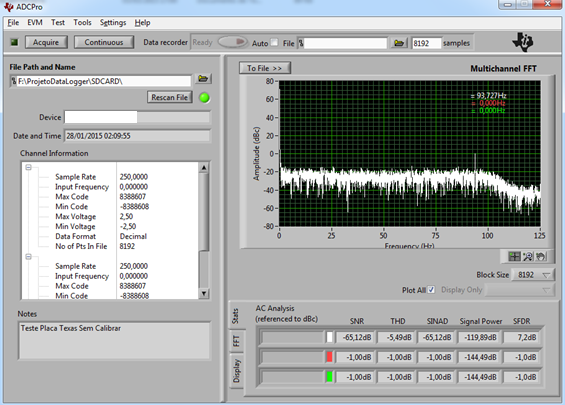
Question 7: When I performed the shorted input tests (250 SPS, unipolar Vref 0 – 5V) at the ADS1282EVM board I reach the following results (Picture 8), Is this correct? Why I have that component at 93.272 Hz? Is it correct the -65,12dB SNR (shorted input it means +2.5V Vocm at the AINP and AINN inputs?)?

                                               Picture 8: AC dBc Analysis ADS1282EVM

The second test I performed after Offset calibration (OFC0 = ADh; OFC1 = FFh; OFC2 =  FFh), no Gain calibration, shorted Pins 2 of S5 and S6. In the next pictures you can see the AC and DC Analysis from the second test.

                                               Picture 9: DC Analysis 2nd test

Picture 10: AC dBc Analysis 2nd test

Picture 11: AC dBFS Analysis 2nd test

The third test I performed after Offset calibration (OFC0 = ADh; OFC1 = FFh; OFC2 =  FFh) and Gain calibration Full Scale, using AVDD supplied by TPS79225 +2.5V(Vref/2) (FSC0 = 35h; FSC1 = D4h; FSC2 =50h).  At this test I just connected the AVDD DC signal directly at the PIN2 of switch S6, and AGND at the PIN2 of switch S5, same procedure for the Full Scale calibration. I also measured the voltage using a true RMS multimeter, after the resistor R51 = 2.451V, before the resistor R51 = 2.495V. In the next pictures you can see the AC and DC Analysis from the third test.

                                                               Picture 12: DC Analysis 3rd test

Question 8: 1513 Codes(pp) it can be considerable a noisy power supply or not for this proposal? 

Picture 13: AC dBc Analysis 3rd test

Picture 14: AC dBFS Analysis 3rd test

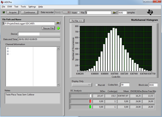
The fourth test I performed after Offset calibration (OFC0 = AAh; OFC1 = FFh; OFC2 =  FFh) and Gain calibration Full Scale, using VREFP supplied by REF5050 +2.5V(Vref/2) (FSC0 = EFh; FSC1 = 4Fh; FSC2 =4Ch).  At this test I just connected the VREFP DC signal directly at the PIN2 of switch S6, and AGND at the PIN2 of switch S5, same procedure for the Full Scale calibration. I also measured the voltage using a true RMS multimeter, after the resistor R51 = 2.196V, before the resistor R51 = 2.222V, this attenuation (2.5V to 2.222V) is mainly caused by the divider network (R57 = 1K and R50 = 10K). In the next pictures you can see the AC and DC Analysis from the fourth test.

Picture 15: DC Analysis 4th test

Question 9: It seems to be very strange but if you compare the Histogram (Picture 15) with the Histogram (Picture 12), show us that the voltage reference supplied by REF5050 has much more noise in comparison to the one supplied by TPS79225. Is this correct? Why?

Picture 16: AC dBc Analysis 4th test

Picture 17: AC dBFS Analysis 4th test

If you need more information let me know, will be a pleasure to share.

Thank you in advance to share your experience!


Best Regards,

Flávio Cavalieri 

  • Hi Flavio,

    Good to hear from you again!

    I'll try to answer all of your questions:

    1. Where do you connect AGND and DGND?

      ...As a minimum, they need to connect below the ADS1282. However, I usually discourage splitting the analog and digital ground planes at all. You've already partitioned your layout such that analog and digital circuits are separated; therefore, analog and digital return currents will naturally remain separated on the same plane.

    2. With a 5V reference, the input range of the ADS1282 is +/-2.5V. Therefore, you 'could' use the PGA with a gain of 2 V/V; however, I would suggest reducing the attenuation to a factor of 1/8. This reduces the size of some of the resistors and results in better overall SNR.

    3. No, I would not use that RC filter. I know you want to filter the reference noise but the ADC's digital filter is already doing most of the noise filtering for you.

    4. I'm looking into this and will get back to you!

    5. a) Make sure that the input common-mode voltage is defined when shorting the inputs. You can short the inputs and connect both to AGND.
      b) Also try using the ADS1282's internal shorts and seeing if this improves the noise. If so, your input circuitry may be contributing to the noise. If still no, then layout is likely affecting the noise performance. I've seen many cases where AGND and DGND were not connected close to the ADS1282 and the noise performance was not the best.

    6. SNR is more applicable when you have an AC input signal present (without a signal it's just a noise ratio "NR"). With the inputs shorted you'll only see a small tone (refer to page 16 of the ADS1282 for details on the tone and its relationship to the input voltage). Figure 1 on page 6 of the datasheet shows the SNR when a nearly full-scale (-0.5 dBFS), 31.25Hz input signal is applied.

    7. The tone is proportional to the input voltage. In this case, with the inputs shorted, the input voltage is simply the PGA's offset. SNR is still bad because there is no applied signal ("S").

    8. Umm... it's hard to tell because you're looking at the combined noise from multiple sources...
      Yes, you are sort of looking at the power supply noise, but you also have reference noise and system noise. Recall that the noise performance was degraded a little with the inputs shorted...that is the best noise performance you can achieve with the ADS1282 in your current system due to the power supplies and layout. When you apply a differential signal (other than 0V), you also see the input signal's noise + the reference noise.

      It is best to use low-noise signal generator to apply a full-scale signal. Then, at least, you reduce the input signal's noise and see mostly just reference noise. But first, you'll want to try to improve the noise when the inputs are shorted.

    9. This is not a standard test and I'm not sure exactly what you could make of it. The REF5050 should have a lower noise than the TPS79225, but by connecting the reference output to the ADC's input, you're coupling the switching current of the ADC's reference input into the ADC's analog input. Recall, how R57 is causing the reference voltage to droop?...The ADC reference input is pulling current!

    Hope that helps!

    Best Regards,
    Chris

  • Hi Christopher,

    It’s good to get your feedback again,

    First of all, thank you very much to spend your time solving my questions.

    Regarding the questions:

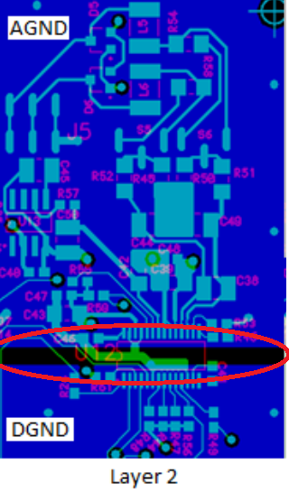
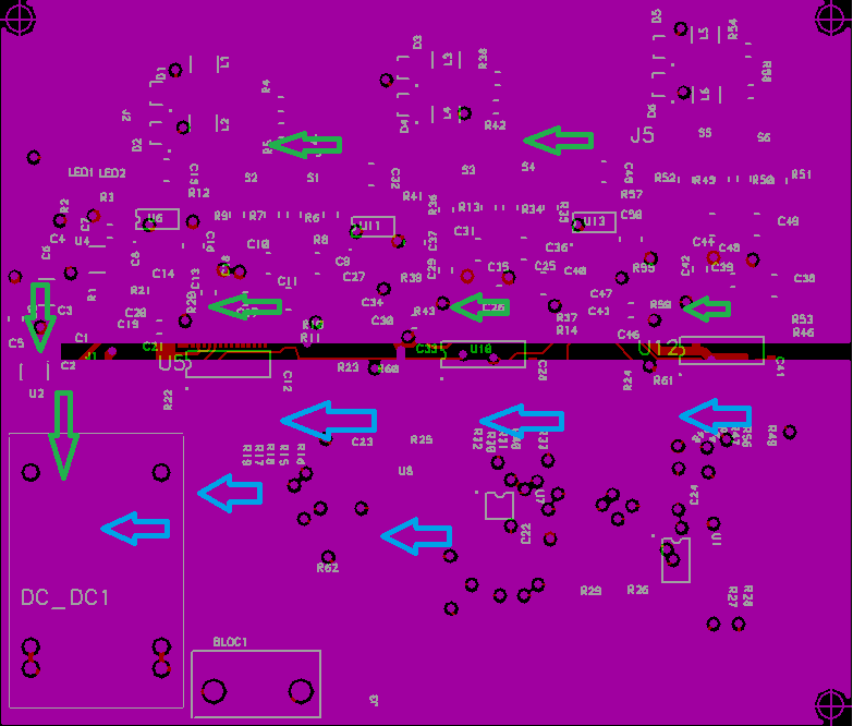
    1-      In the next picture you can see the AGND and DGND layout from the Layer2 (just below the Layer 1), the green arrows represent the current path for the analog ground and the blue arrows represent the current path for the digital ground. You can see the return path in the direction of DC-DC converter GND pin.

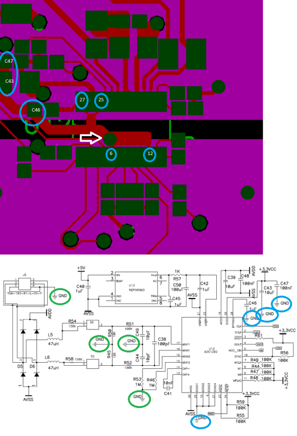
    In the next picture you can see the white arrow indicating a via which connects (ADS1282 DGND pins 25, 27, 6, 12), C47, C43 and C46  to the DGND layer (blue bubbles indicate the pins and components connected to DGND). The green bubbles indicate which components are connected to the analog ground AGND.

    Do you think if I connect AGND and DGND (use a common ground instead of splitting in AGND and DGND) from my actual Layer 2, I can get a better noisy performance?

    2-      I followed you advice and reduced the attenuation to a factor of 1/8.

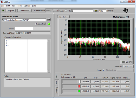
    3..5- I did some tests as you can see by the results in the next pictures:

    Test 1: With RC filter (R57 = 1K, C50 = 100uF), same circuit as the picture bellow:

    This test was done connecting Pins 2 (S6, S5) to AGND (short the inputs and connect both pins to AGND, “connection before R51 and R52”) to make sure that the input common-mode voltage was defined. To proceed with this test I did an Offset calibration!

    Results:

    Test 2: Without RC filter (R57 = 0 ohm, C50 = 1uF), same circuit from the picture bellow:

    This test was done connecting Pins 2 (S6, S5) to AGND (short the inputs and connect both pins to AGND, “connection before R51 and R52”) to make sure that the input common-mode voltage was defined. To proceed with this test I did an Offset calibration!

                    Results:


    Test 3: Without RC filter (R57 = 0 ohm, C50 = 100uF), same procedure as Test 2.

    Results:

                    Test 4: External short, preamplifier inputs shorted  to AINN2 (common-mode test), After the Offset calibration found (OFC0 = D7, OFC1 = FF, OFC2= FF), without RC filter (R57 = 0 ohm, C50 = 100uF).

                    Results:

     Test 5: Preamplifier inputs shorted together through 400Ω internal resistors, After the Offset calibration found (OFC0 = D8, OFC1 = FF, OFC2= FF), without RC filter (R57 = 0 ohm, C50 = 100uF).

                    Results:

    If you compare Test5/Test4 with Test3 we can see an improvement related to the ENOB (lower StDev) but the number of Codes(pp) was worst in comparison to Test3. The Tone is around 2Hz instead of 4Hz from the Test3. Based on these results and your experience with ADS1282 is there something I can change easily in my layout/circuit to try to improve the AD performance?

     6..7: The small tone I can see in the Test 3 (4.050Hz) is related to some PGA’s offset, even after the Offset Calibration? And why 4Hz and not only a DC offset? Should I use 75K resistor like the Picture 70 (Geophone interface application) of ADS1282 datasheet in order to reduce this tone?

    8: Thanks alot for the explanation.

    9: Makes sense, would you recommend me a low-noise signal generator I can use to make the ADC analog input tests?

    Thank you very much Christopher,

    Best Regards,

    Flávio

  • Hi Flavio,

    FlavioCavalieri said:
    Do you think if I connect AGND and DGND (use a common ground instead of splitting in AGND and DGND) from my actual Layer 2, I can get a better noisy performance?

    I think so, but I haven't seen all of your circuitry.

    Typically, the layout recommendation with data converters is to connect the analog and digitial grounds right at the ADC. Connecting them elsewhere on the PCB can cause noise problems.

    One thing to always avoid with split ground planes is routing traces over the split! I see some traces that cross over the ground plane cutout. The return currents for those traces will have to loop around the cutout and will distrubt the return current of other signals (there is a common-impedance noise coupling that occurs). Filling in the ground plane would remove much of this type of noise coupling.


    FlavioCavalieri said:
    If you compare Test5/Test4 with Test3 we can see an improvement related to the ENOB (lower StDev) but the number of Codes(pp) was worst in comparison to Test3. The Tone is around 2Hz instead of 4Hz from the Test3. Based on these results and your experience with ADS1282 is there something I can change easily in my layout/circuit to try to improve the AD performance?

    The difference in noise performance from each of these tests is fairly small. Therefore you cannot be highly certain that there really is a significant difference without performing these tests many more times and averaging the results. Noise is a random variable and it will change slighty each time you collect data. By collecting data only once with each of these configurations, there is a good probability that the randomness of the noise could be misleading. The mean of the noise distributions could very well be equal but you just happen to sample points in different parts of the distributions.

    I don't think the difference in very significant. However, I would make sure to use a value of C50 that is recommened by the REF5050 datasheet. I believe it recommend no more that 50uF.


    FlavioCavalieri said:
    6..7: The small tone I can see in the Test 3 (4.050Hz) is related to some PGA’s offset, even after the Offset Calibration? And why 4Hz and not only a DC offset? Should I use 75K resistor like the Picture 70 (Geophone interface application) of ADS1282 datasheet in order to reduce this tone?

    Yes, the tone frequency is related to the modulator input voltage. Calibration only removes the tone by post-processing the digital information; however, the modulator input still see the offset and produces a tone. As soon as you apply a small signal, the tone's frequency will shift out of the digital filter's passband. Therefore, it is only problematic for near 0V input signals.

    The circuit in figure 70 is an optional way of adding an offset voltage to the modulator to remove the tone when your inputs signal is near 0V. This offset can then be caibrated out of the results.


    FlavioCavalieri said:
    9: Makes sense, would you recommend me a low-noise signal generator I can use to make the ADC analog input tests?

    Typically, the DAC1282 is used as an input to test the ADS1282's performance. You could also use a good bench signal generator, though not all of them will have the THD performance of the ADS1282.

    Best Regards,
    Chris


  • Hi Christopher,

    Thanks again for the fast and precise feedback.

    Regarding the first topic, I'll take care to avoid those traces over the split, in reality the split is located in the Layer 2 (ground planes) and the traces in the Layer 1 (top layer), specially because one of those traces is the SPI DIN line and every 4ms (250SPS) I have data flow from the 3 channel at this line. Should I remove the gap between AGND and DGND and use a complete solid ground at Layer 2? In my board, the analog components (REF5050, Precision Resistors, and so on..) related to the ADC signal inputs are positioned up the ADS1282 (15..28 pins), the digital components (Oscillator, Mux, and so on..) are positioned down the ADS1282 (1..14 pins).

    I'll try to perform more tests and averaging the results. I also changed right now the capacitor C50 value to 10uF.

    In the second board I'll include those 75K resistors in order to make some tests regarding the modulator offset voltage. I'll try to make the traces between the REF5050 and the resistors as short as possible in case we decide to not use the resistors.

    Do you know if Texas has an evaluation board with DAC1282 or other high precision DAC I can use as an input to test the ADS1282 performance?

    Best Regards,

    Flávio
  • Hi Flavio,

    You're welcome!

    FlavioCavalieri said:
    Regarding the first topic, I'll take care to avoid those traces over the split, in reality the split is located in the Layer 2 (ground planes) and the traces in the Layer 1 (top layer), specially because one of those traces is the SPI DIN line and every 4ms (250SPS) I have data flow from the 3 channel at this line. Should I remove the gap between AGND and DGND and use a complete solid ground at Layer 2? In my board, the analog components (REF5050, Precision Resistors, and so on..) related to the ADC signal inputs are positioned up the ADS1282 (15..28 pins), the digital components (Oscillator, Mux, and so on..) are positioned down the ADS1282 (1..14 pins).

    What happens with ground splits or traces on the ground plane, is that return currents get disturbed. They want to follow the return path closest to the sourcing trace, however they are forces around obstacles creating large loops. This may cause noise coupling of various circuits due to a common-impedance path, or worst yet, the current loop may be susceptible to outside noise OR radiate! Here is an example of current loops created by a combination of a ground plane and traces routes on the ground plane :

    Removing the split altogether is usually beneficial, but you'll still need to re-evaluate the new return current paths to make sure analog and digital return currents are not overlapping (and coupling digital noise into the analog circuitry through a common-impedance).

    You've already partitioned the analog and digital circuitry into different regions on your PCB, so it is unlikely that you'll have many digital signals with return current path common to an analog signal return current path - but double check anyways!


    FlavioCavalieri said:
    Do you know if Texas has an evaluation board with DAC1282 or other high precision DAC I can use as an input to test the ADS1282 performance?

    Unfortunately we don't have an evaluation board for the DAC1282.

    Do you have any good bench signal generators available to you?


    Best Regards,
    Chris


  • Hi Christopher,

    Thanks for sharing this information, I'll try to follow your advices during the newer layout for the second PCB.

    Regarding the signal generators we have, unfortunately it should be not enough (Range 2m Vpp to 20 Vpp, Amplitude resolution = 8 bits), Could you recomend me a good one I can use here to evaluate the boards?

    Just to share a newer information, we did some tests now with the 3 Channels, working at the same time, and got the following results (no offset/gain calibration):

    Best Regards,

    Flávio

  • Hi Flavio,

    Something like an Audio Precision or Keysight 33xxx signal generator would probably work well for you. There may be other good options, I'm just familiar with these ones.

    Best Regards,
    Chris

  • Hi Christopher,

    I'll try to find an option like the ones you told me.
    I just have two more questions:

    1- Have you found something regarding the 32bit variable reading in the ADCPro?
    2- In my application I'm using Linear Phase Filter settings, whats the real delay I have to consider when I record the filtered values? it's the group delay 31/fdata in my case 31/250SPS = 124 ms? So it means my actual filtered value represents an analog value applied 124 ms before in the PGA inputs?

    Best Regards,

    Flávio
  • Flavio,


    1 - We may have a fix for the 32 bit reading for ADCPro. If you are interested, may we contact you by email for the solution?

    2 - The real delay that you need to consider is not the group delay, but rather the settling time. This would be 62/fdata. For your case, this would be about 248ms to get fully settled data.


    Joseph Wu
  • Hi Joseph,

    First of all thanks for the reply,

    1- Yes, please.
    2- I found this value in the ADS1282 datasheet page 24, (62.98046875/fDATA + 468/fCLK), is this the real delay I have to consider (aprox.: 63//fDATA )?

    Best Regards,

    Flávio
  • Flavio,


    1. We'll contact you soon.

    2. The delay of 62 data periods should be correct. The 62.98046875/fDATA + 468/fCLK number occurs when there are other ADC setups involved. In the datasheet, the equation is used when there is Pulse-Sync, Reset pin toggle, Reset command, or Power-on/Wake-up. For each of these, there is additional setup/delay associated with the digital section of the ADC. However, if it's easier, use the 63 data periods for your delay.


    Joseph Wu
  • Hi Joseph,

    Thanks again for the fast reply.

    As I understood The delay of 62 data periods is the one I should use in my application? My configuration values for CONFIG0 and CONFIG1 registers are respectively 0x42 and 0x08. This is very important because in my application each sample has to provide also precise time stamp information.

    Best Regards,

    Flávio
  • Flavio,


    The 62.98046875/fDATA + 468/fCLK is applicable only for the first conversion after one of a few types of events.

    If you are starting and restarting your ADC, through either a reset, pulse sync, or power-down, power-up, then you would need to wait for 62.98046875/fDATA + 468/fCLK to see the first /DRDY indication. After that, the data comes out at the 1/fDATA period.

    The point of this equation is that each time the device is restarted from one of these events, the first data coming out will be settled and will take a bit longer than the expected 62/fDATA for settling.

    If you have more questions about the nature of the delay, it might help to know how you intend to use the device, if you intend to start and restart the ADC, and what it is your are reading.


    Joseph Wu
  • Hi Joseph,

    I think it's clear now.

    As I understood the 63/fDATA is only the settling time for the first conversion, in my case I used a pulse sync event to synchronize my channels. The DRDY signal generates an interruption in my microcontroller, so every single interruption I record the analog value and also a time stamp.

    To verify the group delay (32/fData - Linear Phase Filter), I set one of the available digital outputs to change their status right after the first DRDY interruption, the 3.3V signal was exactly readable after (32/fData = 128ms) as you can see in the following picture:

    This means when a transaction from 0V to 3.3V occur at 13:51:43,118 it will be only available in the ADS1282 SPI output 128ms later (13:51:43,246), so can I conclude the analog value available at 13:51:43,118 (first DRDY transaction after sync event) is in reality the analog value present in the ADS AINP AINN inputs 128ms before (13:51:42,990)?

    Best Regards

    Flávio

  • Flavio,


    That's basically correct. The group delay would cause the SPI reading to be seen at basically 32/fData after the analog value. However, note that for a step response, the settling time would be 63/fData to get to final value.

    This is shown in the same way in Figure 43 in the datasheet (for the Linear Phase Filter).


    Joseph Wu