This thread has been locked.

If you have a related question, please click the "Ask a related question" button in the top right corner. The newly created question will be automatically linked to this question.

ADS1298 WREG in CONFIG1 problem

Other Parts Discussed in Thread: ADS1298

Hello, I´m trying to change the value of the CONFIG1 register once it has been initialized to another value, but everytime I try to change its value all the registers turns their value to 0 (including CONFG1 register).

A Scheme:

Initialization:

WREG(CONFIG1)--> A6

Later, inside the main loop of my program:

RREG(CONFIG1) =A6

WREG(CONFIG1)-->A5

RREG(CONFIG1) = 0

RREG(CHANNEL2) =0

...

Could you please tell me where could be the problem?

I can change any ohter register without problem, but everytime I change CONFIG1 all the registers turn to 0.


Thank you very much

I hope to hear from you soon.

Best Regards

  • Hello Al,

    Are you issuing the SDATAC command or stopping the converter in some way before re-configuring the registers? It's possible that your timing is such that when you try to read from or write to the CONFIG1 register during the main loop of your program that the DRDY pin falls low and interrupts the RREG or WREG transaction with new conversion data. In that case, whatever data that gets shifted in after DRDY falls low would be latched into the device and it may not be your intended command. If you believe your timing should be fine, post some oscilloscope screen captures of those register reads and writes (SCLK, CS, DIN, DOUT, DRDY) so we can examine it more closely.

    Regards,
    Brian Pisani
  • Hello Brian, thanks for your response,

    Yes I do, I always send SDATAC command before WREG command. I´ve seen that DRDY is always  HIGH, and the other registers can be written without any problem.

    That´s the reason why I think that it could not be a SPI communication problem.

    Best Regards,

    Sixto

  • Hey Al,

    What else happens to the device after the failed WREG? Are you able to read conversion data? If you start the converter again, does DRDY begin to pulse? If DRDY continues to pulse, at what rate does it do so? I'm asking so I can find out what sort of state the device is in after the failed read. Plus I noticed your write to the CONFIG1 register is to change the datarate from 250 SPS to 500 SPS so the rate that DRDY pulses will reveal the true contents of that register. If that register did actually change to 0x00 and you can see DRDY pulse, then it should be happening every 62.5 microseconds. If you cannot see DRDY, then check the CLK pin. It should no longer be outputting the internally generated clock if that register got set to 0x00. If all the other registers got changed to 0x00 as well, then the internal reference should no longer be functioning properly (if you are using the internal reference). If possible, check the internally generated reference voltage and see if it is clean and at the expected voltage.

    Regards,
    Brian Pisani
  • Hello Brian

    Thanks for your answer.

    I´ve been checking all the pins that you´ve mentioned.

    When I rewrite CONFIG1 register ( therefore all the registers are turned to zero)  and I send the RDATAC command. It seems like there is not any variation in DRDY  signal. Therefore I can not catch any data from ADS1298.
     Nevertheless, I can chack CLK internal signal ( pin 37) is ON. and Vref (pin 24) is 2.4v.


    Thank you very much for your help,

    Best Regards


  • Hi Al,


    From what you’ve described, the analog functionality of the device hasn’t changed (the reference and clock output are still behaving normally). We can narrow down the issue to a few possible areas. The problem is probably an issue with the digital functionality of the device (such as the device is entering a reset or power-down state), an SPI communication issue, or a software issue. You’ve said you don’t think your SPI communication is the problem since you’ve been able to read and write other registers successfully without issue. Take a look at your pin connections on the device and make sure there is nothing that could trigger a reset.


    To narrow the problem further, I’d be interested to know if you’ve verified the MISO output in any other means besides through the use of your software. Have you looked at the SPI transactions on the oscilloscope? It is sometimes helpful to look at the data coming back as a sanity check before looking deeper into the problem. If you’ve looked at the successive SPI transactions starting with your RREG command before the CONFIG1 write that causes the problem and the data is definitely coming back as zeros, let me know. Meanwhile, I will talk with the designers to see if there is some other way that the communication would stop like that.


    Regards,

    Brian Pisani

  • Hello Brian,

    Thank you very much for your replies, You are helping me a lot with this problem.

    RESET pin is allways connected to VDD, in this way, my ADS1298 will never suffer a hardware RESET.

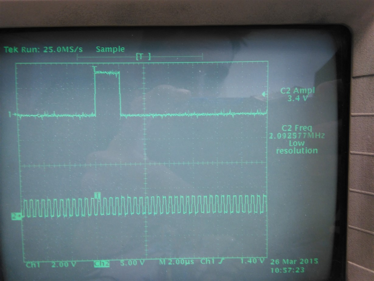
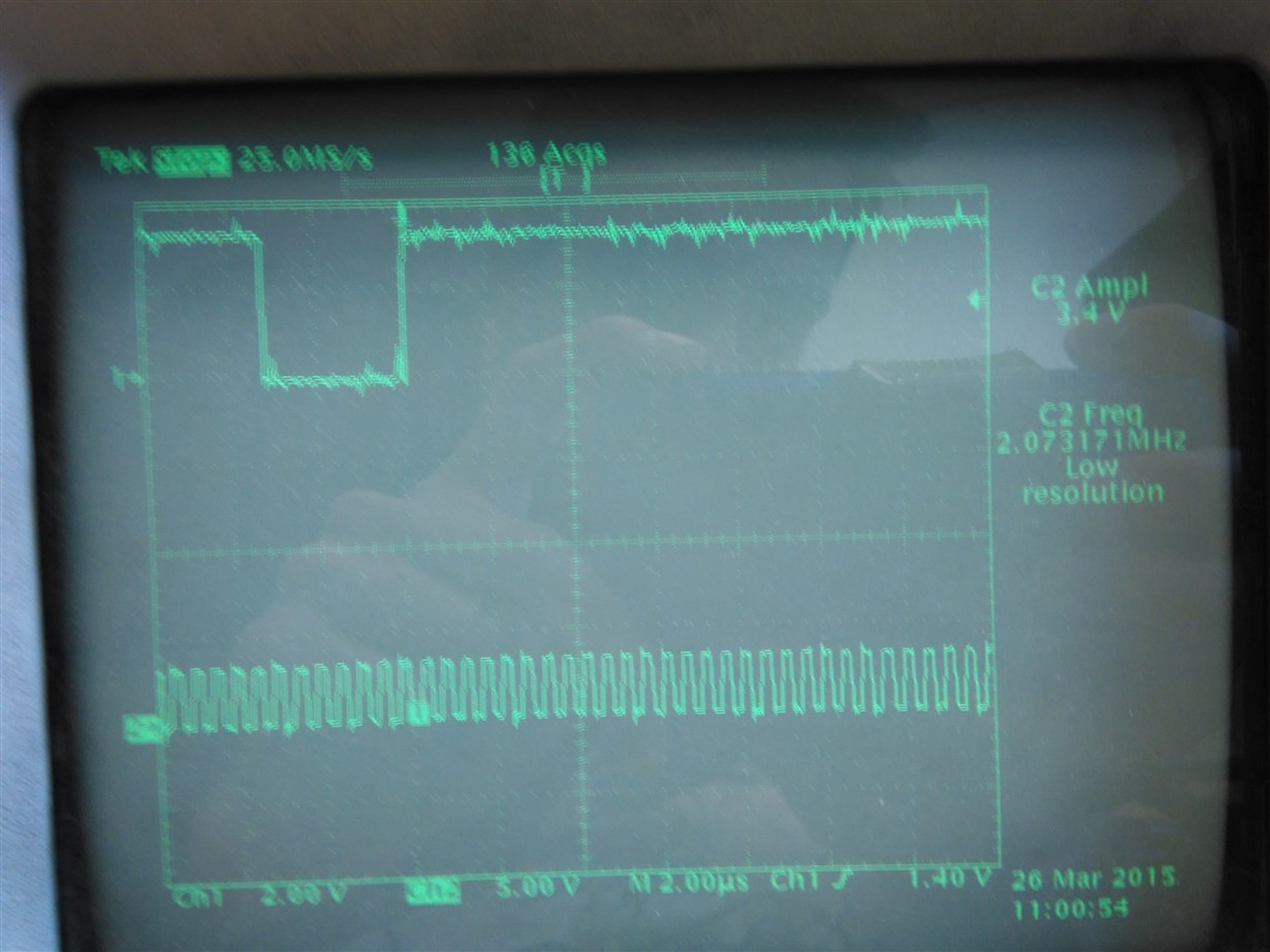
    I have been looking at SPI signals with the oscilloscope, and I have noticed that when I rewrite CONFIG1 register, SCLK signal´s amplitude decrease from 3.28V to 1.20 V.

    These  are the signals in SCLK and DOUT  (DIN in my microcontroller) when I send a RREG(address 0x05)  before and after rewrite the CONFIG1 register

  • Hello Al,

    This definitely seems like a hardware issue. Something you said a few posts ago caught my attention. You said that DRDY always remains high at least at some point in the timeline of your routine. Does it ever fall low? The SDATAC command shouldn't stop the converter (which in turn should not stop DRDY from indicating new conversions), it just prevents conversion data from disrupting other SPI communication processes. Perhaps try holding the START pin high and see if conversions continue even following the event which causes the device to become unresponsive.

    You indicated that RESET is always held high, but I would also recommend looking at the status of the PWDN pin during that RREG and WREG to the CONFIG1 register. Out of curiosity, have you tried pulsing the RESET pin following the shut down in communication to see if the device recovers?

    Finally, are you following the power up sequence specified on page 42 of the ADS1298 datasheet? Following that sequence ensures that the digital portion of the device is initialized correctly.

    Regards,
    Brian
  • Hello, I apologise for the delay. I have been working on another issues of my Master thesis these 3 days.

    Yes, DRDY is always high. There is not any pulse in this line when Isend WREG(CONFIG1) command.

    PWDN* PIN is always HIGH

    I have put START pin HIGH but nothing has changed.

    Another question, Is it necessary to do anything else when I send a WREG(CONFIG1)? like a reset or a start command?

    I can not try pulsing RESET pin because in my PCB is directly connected to DVDD. I think that this could be the problem, as I have connected RESET to DVDD it is impossible for this line to have a LOW pulse like pulse shown on page 42 of the ADS1298. Nevertheless the other registers works fine. That was the reason I was not worried about the reset pin and I though the initialization was OK , but now I think that having RESET pin connected to DVD could be a problem.

    I have tried a software RESET + START but I dont have any response... which have sense because SPI communication seems to be inoperative.

    Thanks for your help,

    Best regards
  • I have just tried sending a RESET+delay+ START from my microcontroller everytime I write in CONFIG1 register, but It continues sending me zeroes in every read command I send (of course I have tried to rewrite these registers that I read before I send the read command).. Please Help!

  • Hey Al,

    I doubt that the RESET pin being pulled high is the reason that the device is not behaving as expected. Issuing the RESET command instead of hitting the RESET pin during the startup routine is a valid sequence. There should be no need to issue any more commands when addressing the CONFIG1 register. Does the DRDY pin ever pulse when the START pin is high? You said your SCLK logic level drops after the WREG to CONFIG1. Does the modulator clock output also drop in logic level after that register write? Does the CLK frequency change at all?

    Brian
  • Hello Brian, Thanks for your help again .

    When I switch on my device  and I put START pin HIGH a pulse appears in DRDY line, when I put START pin low this pulse dissapear and DRDY goes LOW (I think that is strange). when I start a conversion (I send RDATAC, read and send SDATAC to stop the conversion) a pulse appears in DRDY and it keeps in this way always although I send a SDATAC command. Nevertheless when I write CONFIG1 register and I put START pin up DRDY goes high and it does not change.

        I dont have a pulldown resistor connected in this pin, but I have a pull-up resistor connected on DRDY line.

    THere is no variation in CLK signal, it is always maitaned at 2 MHz with 3.4 Volts.

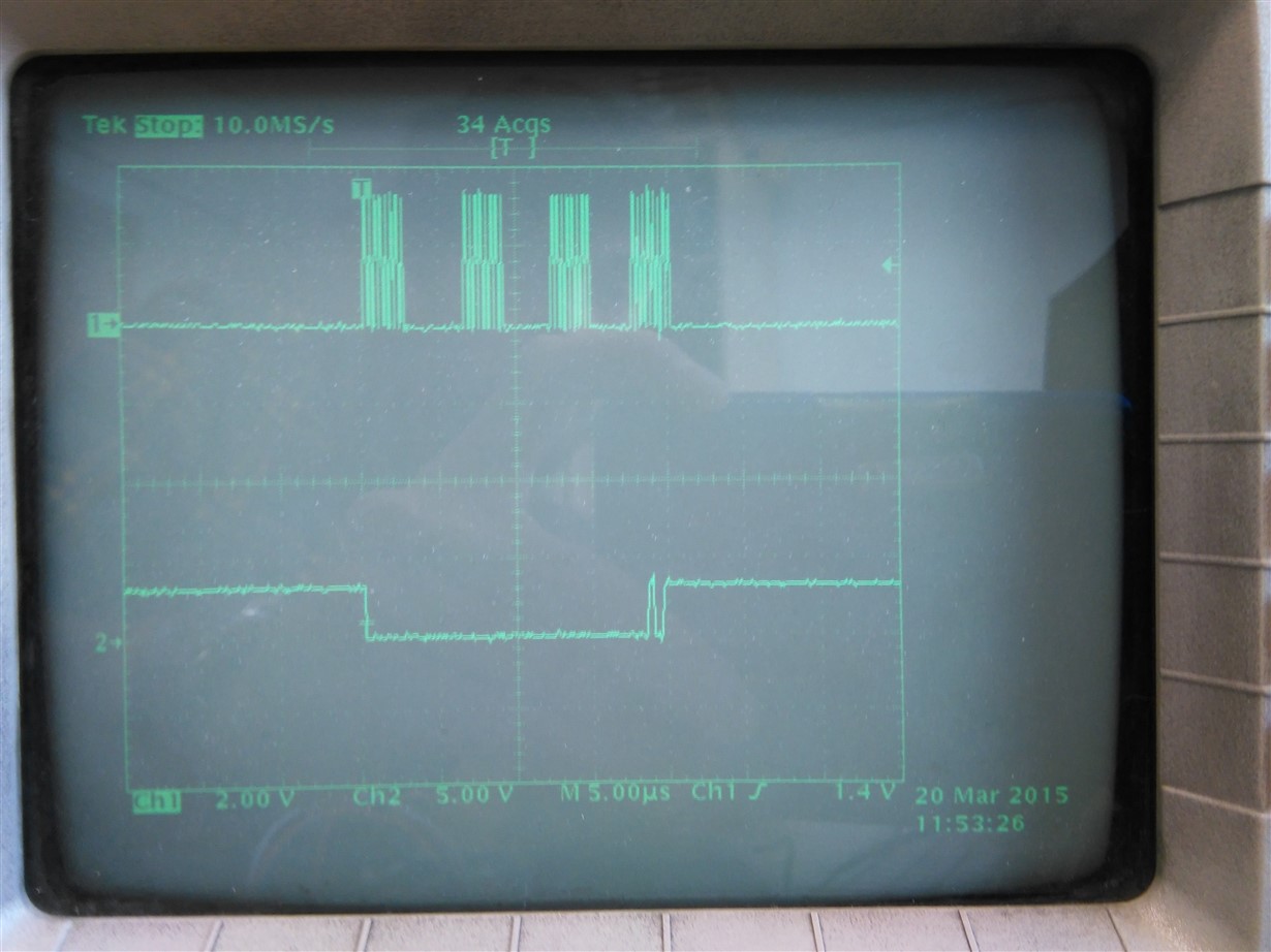
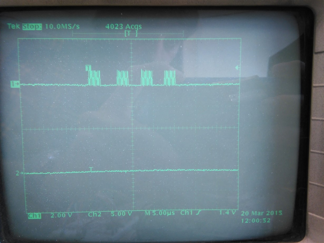
    I am sending you some photos

    -At the beggining  DRDY and CLK

    -While it is reading from the ADS, DRDY and CLK

    when I have sent  WREG(CONFIG1)

  • Hi Al,


    It almost seems like the digital side of the device is shutting down, but the analog side is staying totally active. Very strange behavior! Would you mind sending me your schematic to look at?


    When DRDY is low after the START pin is pulled low, it only means that there was new conversion data ready but not read at the time the converter was stopped. This is normal behavior. Sending the SDATAC command does not stop the converter and as such will not stop DRDY from pulsing.  The SDATAC command simply stops the new conversion data from being automatically loaded into the device output shift register which would otherwise interrupt a register read or write. Remember that data can be read out on command when the converter is in SDATAC mode. In that mode, conversion data will only be shifted out of the device when the converter receives a RDATA command.


    To test the power supply for the digital functionality, I’d like you to probe DVDD before and after the shutdown event and see if the voltage has changed. Would it also be possible for you to monitor current on that line?


    The pullup resistor on the DRDY pin is unnecessary and is known to cause unwanted power draining when it is pulled up or down. Remove that resistor and probe it after the shutdown event and see if the behavior or voltage is different.


    Regards,

    Brian Pisani

  • Hello Brian,

    I have checked AVDD and DVDD after and before I send the command, and there is no variation in the voltage ( AVDD =3V DVDD= 3.3V ). I can not monitor current in my circuit. I have not any resistor to probe the current.

    I have removed pullup resistor in DRDY line but there is no variation.


    I enclose the schematic.

    Thanks for your help Brian.

    Best Regards,

    Sixto

  • Hi Al,

    Are you attempting to activate that diode connected to GPIO4 at any point? If we assume the diode has a junction voltage of 2.5 V when activated, then we can expect it to demand a current of ~5mA across the 150 Ohm resistor. This current is much higher than the rated output current for a digital output on this device. I recommend configuring that GPIO as an input for now to disable the GPIO output buffer. In addition, what is the state of GPIO1? Unused GPIOs should be tied low and configured as inputs (GPIO pins are configured as inputs by default).

    Regards,
    Brian
  • Hi Brian,
    Initially I put this LED in th GPIO4 as a "debug LED", but I´m not using it .
    I will remove both of them in the next design.
    Thanks

    Regards
  • Hey Al,

    Would you mind sending me an email so we can take this conversation off the forum? Your issue seems to be very case specific and I'd be happy to continue to help you over email if necessary. My email address is b-pisani@ti.com.

    Thanks,
    Brian
  • There is a solution of this problem? I have the same!!!