This thread has been locked.

If you have a related question, please click the "Ask a related question" button in the top right corner. The newly created question will be automatically linked to this question.

AMC7812 - Can't write to or read from registers

Other Parts Discussed in Thread: MSP430G2553, AMC7812

Hello,


I’m having issues interfacing with the AMC7812. It’s connected using an SPI interface with a MSP430G2553 CPU. The MSP430G2553 CPU is on a TI Launchpad MSP-EXP430G2 PCB, which is powered over USB but has been modified such that it uses 3.3 V rather than 3.6 V. The SPI_SCK, SPI_MOSI, SPI_MISO, SPI_NSS, RESET and GND of the TI Launchpad PCB are connected using a short cable (approximately 10 cm) to the PCB with the AMC7812 on it.

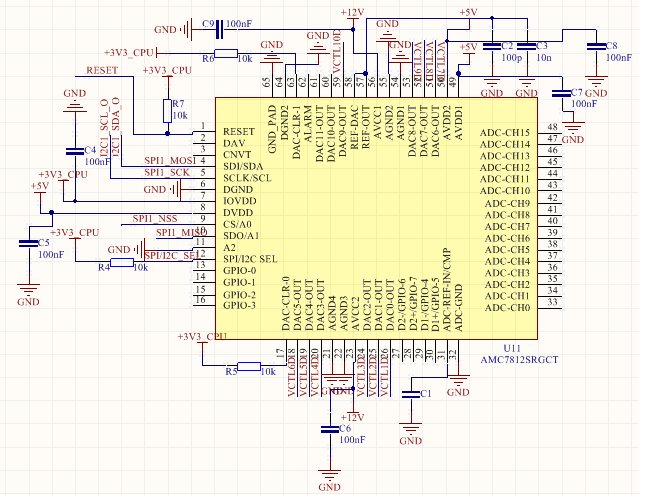
The schematic for the AMC7812 section of the circuit is as follows:


The code I am using on the MSP430G2553 CPU to control it is as follows:

/*

* main.c

*/


#include <msp430.h>

#include <msp430g2553.h>

#include <stdio.h>


unsigned char address_read;

unsigned char databyte1_read;

unsigned char databyte2_read;


void clockConfig()

{

// configure the CPU clock (MCLK)

// to run from DCO @ 16MHz and SMCLK = DCO / 4

BCSCTL1 = CALBC1_16MHZ; // Set DCO

DCOCTL = CALDCO_16MHZ;

BCSCTL2= DIVS_3 + DIVM_0; // divider=4 for SMCLK and 1 for MCLK

}


void pinConfig()

{

// set the pin mode 3 for pins 1, 2, 4 of port 1 (USCI mode)

P1SEL = BIT1 + BIT2 + BIT4; // low bit = 1 for pin 1, 2, 4

P1SEL2 = BIT1 + BIT2 + BIT4; // high bit = 1 for pin 1, 2, 4


P1DIR |= BIT3 + BIT5; // p1.3 and p1.5 set to output to drive RESET and CS

P1OUT |= BIT3 + BIT5; // pull p1.3 and p1.5 to high - RESET and CS high

}


// USCI

void spiConfig()

{

UCA0CTL0 |= UCMSB + UCMST + UCMODE_0 + UCSYNC;

// synchronous (=SPI) master 3 wire SPI, clock polarity low

/*SPI mode is selected when the UCSYNC bit is set and SPI

mode (3-pin or 4-pin) is selected with the UCMODEx bits, i.e.

slave enabled when UCxSTE pin is low.*/

//use SCLK : 4MHz

UCA0CTL1 |= UCSSEL_2;

// set baud rate = SMCLK, no further division

UCA0BR0 = 0;

UCA0BR1 = 0;

UCA0MCTL = 0; // No modulation

UCA0CTL1 &= ~UCSWRST; // **Initialize USCI **

}


// sets a register of the TI AMC7812 Multichannel ADC/DAC via SPI

void setRegisterValue(unsigned char address, unsigned char databyte1, unsigned char databyte2)

{

       P1OUT &= (~BIT5);   // Select Device

//     __delay_cycles(10);


       UCA0TXBUF = address; // Send address register byte

       while (!(IFG2 & UCA0TXIFG)); // wait for TX buffer ready

       UCA0TXBUF = databyte1; // Send data byte 1


       while (!(IFG2 & UCA0TXIFG)); // wait for TX buffer ready

       UCA0TXBUF = databyte2; // Send data byte 2


       while (!(IFG2 & UCA0TXIFG)); // wait for TX buffer ready

              __delay_cycles(70);

              P1OUT |= (BIT5); // Unselect   Device


              __delay_cycles(146200);

}


void powerdacConfig()

{

       __delay_cycles(400000);

       P1OUT &= ~BIT3; // pull p1.3 to low - RESET low

       __delay_cycles(400000);

       P1OUT |= BIT3; // pull p1.3 to high - RESET high

       __delay_cycles(400000);


       setRegisterValue(0x6B, 0x3F, 0xF8); // Write to Power-down register - turn on Internal Reference and DACs 0-9

       setRegisterValue(0xEB, 0x00, 0x00); // Read from Power-down register

       setRegisterValue(0x59, 0x03, 0xFF); // Write to DAC gain register - set DAC 0-9 gain bits to 1

       setRegisterValue(0x58, 0x03, 0xFF); // Write to DAC config register - enable sync. load for DACs 0-9

}


void loadData()

{

       setRegisterValue(0xEC, 0x00, 0x00); // Read from device ID register

       setRegisterValue(0x33, 0x08, 0x00); // Write to DAC 0 data register - set to 2048/4096 counts = 6 V

       setRegisterValue(0xB3, 0x00, 0x00); // Read from DAC 0 data register - set to 2048/4096 counts = 6 V

       setRegisterValue(0x34, 0x08, 0x00); // Write to DAC 1 data register - set to 2048/4096 counts = 6 V

       setRegisterValue(0x35, 0x08, 0x00); // Write to DAC 2 data register - set to 2048/4096 counts = 6 V

       setRegisterValue(0x36, 0x08, 0x00); // Write to DAC 3 data register - set to 2048/4096 counts = 6 V

       setRegisterValue(0x37, 0x08, 0x00); // Write to DAC 4 data register - set to 2048/4096 counts = 6 V

       setRegisterValue(0x38, 0x08, 0x00); // Write to DAC 5 data register - set to 2048/4096 counts = 6 V

       setRegisterValue(0x39, 0x08, 0x00); // Write to DAC 6 data register - set to 2048/4096 counts = 6 V

       setRegisterValue(0x3A, 0x08, 0x00); // Write to DAC 7 data register - set to 2048/4096 counts = 6 V

       setRegisterValue(0x3B, 0x08, 0x00); // Write to DAC 8 data register - set to 2048/4096 counts = 6 V

       setRegisterValue(0x3C, 0x08, 0x00); // Write to DAC 9 data register - set to 2048/4096 counts = 6 V

       setRegisterValue(0x4C, 0x0C, 0x00); // Write to AMC config register - activate sync. load for DACs 0-9

       __delay_cycles(14600000);

}


int main(void) {

// setup

WDTCTL = WDTPW | WDTHOLD;

clockConfig();

pinConfig();

spiConfig();


int i=0;


while(1)

{

//__delay_cycles(14600000);

powerdacConfig();

loadData();

if ( i == 0 ) break; // for an example.

i++;

}


while(1)

{

//__delay_cycles(73000000);

loadData();

//if ( i == 0 ) break; // for an example.

//i++;

}

}


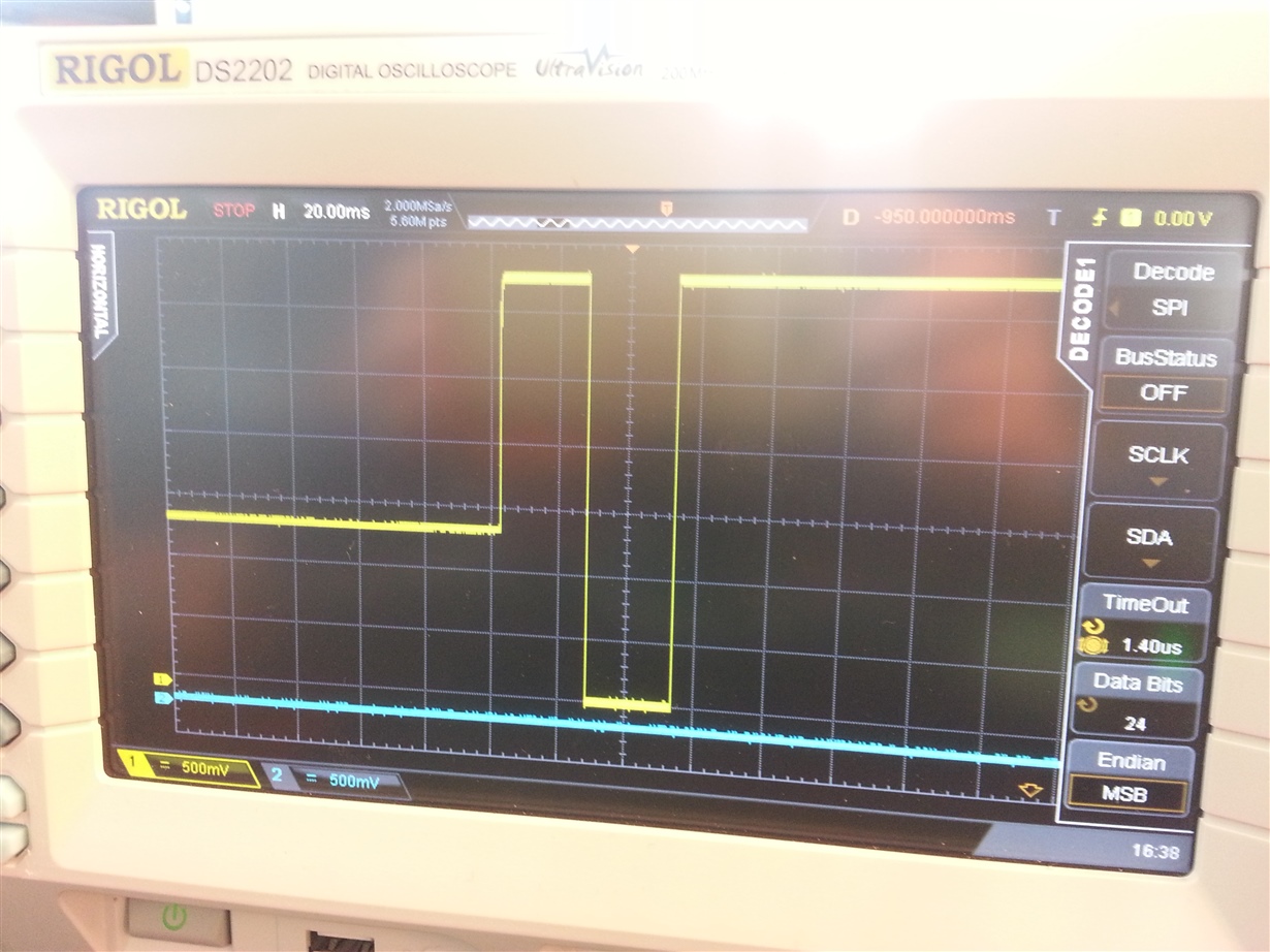
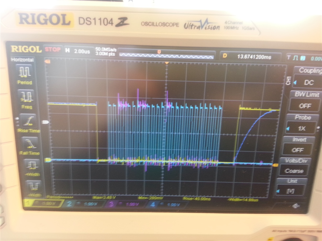
As you can see the RESET pin is high at power-up and is then pulled low after 27 mS before being pulled high again after a further 27 mS. Then there is a 27 mS delay before I start writing to or reading from registers on the AMC7812. Firstly I write to the power-down register, to activate the internal reference and DACs 0-9, then I try to read the device ID, then I write to the DAC gain and configuration registers. There is then an infinite loop, with approximately 1 second delay between each cycle, whereby I try to read the device ID register first and then load data into DACs 0-9 and synchronously update it using the AMC configuration register.

The problem is that I can’t read the device ID and the internal reference and DAC 0-9 outputs are all at 0 V. I’ve taken screenshots below using the oscilloscope of what is happening when I try to read the device ID:

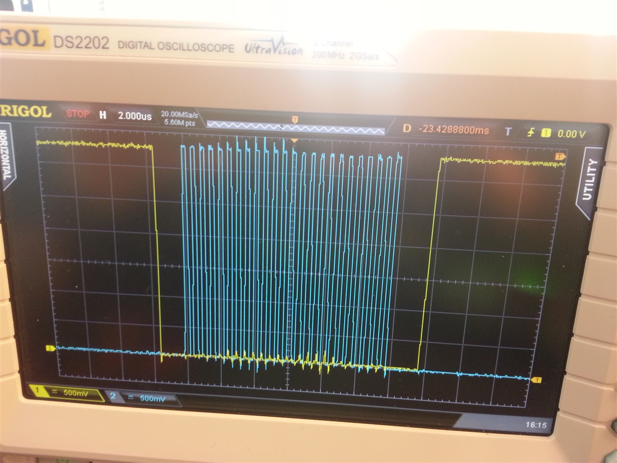
  1. SPI_NSS, SPI_SCK – exactly 24 clock cycles occur between when the chip select is pulled low and when it goes high again. I am using a 4 MHz clock for the SPI. There is more than adequate delay between when chip select goes low and the clock starting and also between when the clock ends and when chip select goes high.

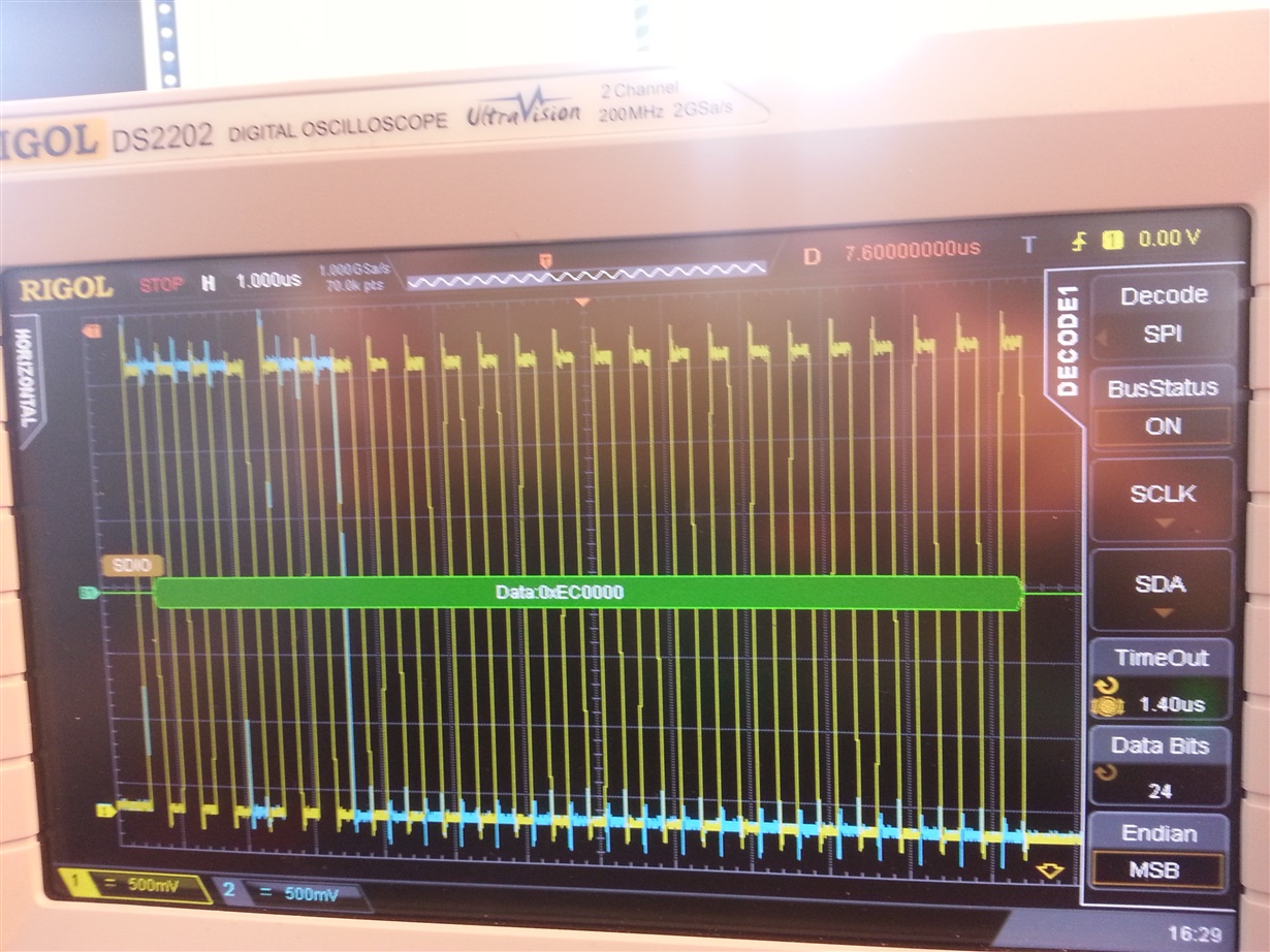
2. SPI_SCK, SPI_MOSI – as you can see the oscilloscope’s SPI decode function is able to decode the transmission successfully, i.e. 0xEC 0x00 0x00.


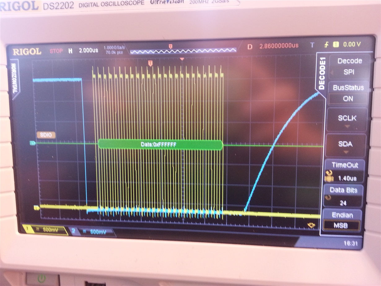
3. SPI_SCK, SPI_MISO – this is taken from the CS-active period after the above one, i.e. when the AMC7812 should output the device ID from the 0x6C register. The MISO line is pulled low but then stays low for the duration of the CS-active period.


I have also taken a screenshot using the oscilloscope of what happens to the RESET pin at startup, as you can see it starts off at a floating voltage of approximately 1.3 V (as the MSP430G2553 is powered up after the AMC7812 voltage rails), then within 27 mS of power-on it is pulled low for 27 mS before being pulled high again:


I have arranged for the AMC7812 IC to be replaced on our PCB, to see if it has been damaged in some way or if it’s not fitted correctly on the PCB. The pin 1 marker is in the right location and as far as I can tell all the pins of the IC are connected to the pads on the PCB. You help would be much appreciated!

  • Hi Peter,

    Thank you for the post and all the information.  I've looked over your schematic, and I don't see anything that stands out.  The one thing I am curious about is the state of the SDI signal in your second frame.  Is it possible to retake the above oscilloscope capture with the following 3 signals (SDI, SDO, and SCLK)?  Reducing the scale of the amplitude, via oscilloscope, will also help make the signals more readable.

    In summary, the SPI read is broken down into two frames.  The table below illustrates the correct procedure for a read operation:

    You must still write 0xEC to SDI in the second frame of the read.  You may be doing this, but it is unclear from your capture since SDI is not included.

    An oscilloscope capture of both frames with all three signals would be helpful.

    Best Regards,

    Matt


  • Hi Peter,

    I think I may have spoken too soon regarding the schematic.  Your current schematic may still be acceptable for your current application, but I just wanted to note potential problems.

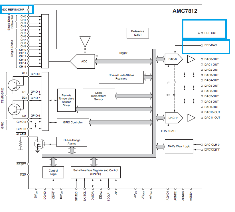
    The schematic you've included connects REF-OUT and REF-DAC to 5V.  REF-OUT outputs 2.5V when the bit PREF is set to '1'.  You must always ensure that the internal reference is not used, PREF set to '0', otherwise the supplies will short, which can damage the internal reference block.

    There is also  no external reference supplied to ADC-REF-IN and since you can't use the internal reference, this basically takes the ADC block out of the equation.  You don't seem to be using any of the ADC inputs in your schematic, so you may be ok.

    If you wish to use the ADC inputs in future applications, you may want to change your design.  I've included the block diagram of the AMC7812 for reference.

    Best Regards,

    Matt

  • Hi Matt,


    Many thanks for your replies, we have a 4-channel oscilloscope also (albeit with no SPI decode function) so I used that to take some oscilloscope captures of frame 1, frame 2 and frame 3 of the 'loadData' function in the above code. I rewrote this section of the code to use 2 consecutive read transmissions when I'm reading the device ID, I hadn't noticed that requirement in the datasheet:

    void loadData()
    {
         setRegisterValue(0xEC, 0x00, 0x00); // Read from device ID register
         setRegisterValue(0xEC, 0x00, 0x00); // Read from device ID register
         setRegisterValue(0x33, 0x08, 0x00); // Write to DAC 0 data register - set to 2048/4096 counts = 6 V
         setRegisterValue(0xB3, 0x00, 0x00); // Read from DAC 0 data register - set to 2048/4096 counts = 6 V
         setRegisterValue(0xB3, 0x00, 0x00); // Read from DAC 0 data register - set to 2048/4096 counts = 6 V
         setRegisterValue(0x34, 0x08, 0x00); // Write to DAC 1 data register - set to 2048/4096 counts = 6 V
         setRegisterValue(0x35, 0x08, 0x00); // Write to DAC 2 data register - set to 2048/4096 counts = 6 V
         setRegisterValue(0x36, 0x08, 0x00); // Write to DAC 3 data register - set to 2048/4096 counts = 6 V
         setRegisterValue(0x37, 0x08, 0x00); // Write to DAC 4 data register - set to 2048/4096 counts = 6 V
         setRegisterValue(0x38, 0x08, 0x00); // Write to DAC 5 data register - set to 2048/4096 counts = 6 V
         setRegisterValue(0x39, 0x08, 0x00); // Write to DAC 6 data register - set to 2048/4096 counts = 6 V
         setRegisterValue(0x3A, 0x08, 0x00); // Write to DAC 7 data register - set to 2048/4096 counts = 6 V
         setRegisterValue(0x3B, 0x08, 0x00); // Write to DAC 8 data register - set to 2048/4096 counts = 6 V
         setRegisterValue(0x3C, 0x08, 0x00); // Write to DAC 9 data register - set to 2048/4096 counts = 6 V
         setRegisterValue(0x4C, 0x0C, 0x00); // Write to AMC config register - activate sync. load for DACs 0-9
         __delay_cycles(14600000);
    }

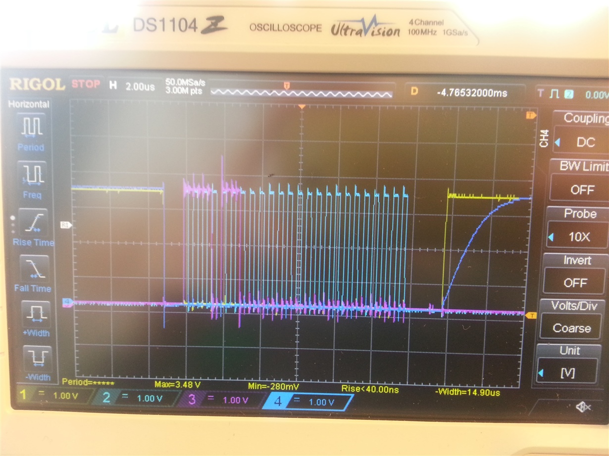
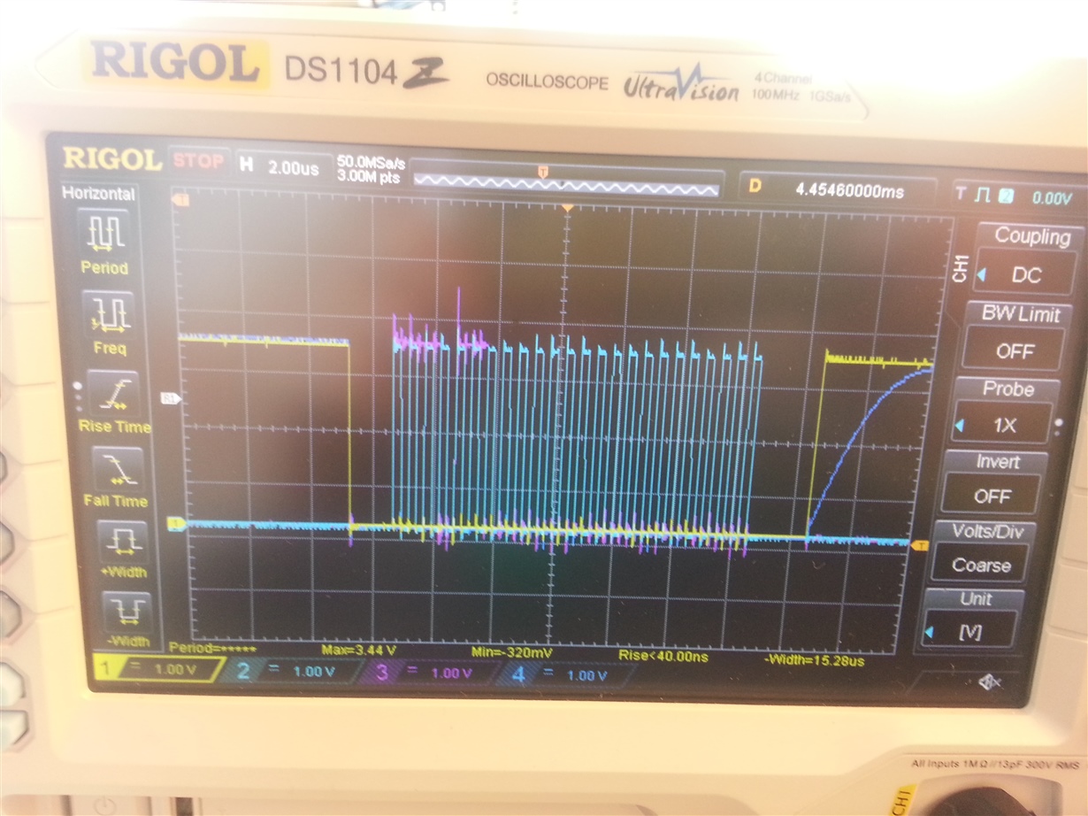
    The oscilloscope captures for frames 1-3 are as follows, note that Channel 1 = CS, 2 = SCLK, 3 = SDI (MOSI), 4 = SDO (MISO):

    As you can see the SDO trace still goes to 0 V for the duration of each frame, apologies if the colours of channels 2/4 are quite similar but there doesn't seem to be a way to change them.

    With regard to the REF-OUT and REF-DAC traces in the schematic I posted, they're not actually connected to 5 V, it looks like they do I know but it's just the way the schematic is drawn, the 5 V supply is just connected to AVDD2, I've checked in the layout to be sure also.

    I'm beginning to think that the DAC IC has been damaged in some way, I should be getting back some PCBs this week with replacement ICs fitted so that may help shed some light on what's happening.

  • Hi Peter,

    Thanks for the captures.  Can you confirm the voltage levels on the supply pins?  These are the IOVDD, DVDD, AVDD and AVCC pins.  

    As you may know with SPI there are two options known as CPOL and CPHA.  These values specify the base value of the clock and whether data is captured on the rising or falling edge of SCLK.

    It is still somewhat difficult to view from the capture, but I'm assuming that you are implementing a clock polarity of 0,  and clock phase of 1.   These values correspond to a clock base value of 0, and data is captured on the clock's falling edge, which should be correct for communication with the AMC7812 device.  Can you confirm this?

    You can perform this by staggering the input channels of the oscilloscope capture, and by also decreasing the amplitude of the signals.  This will allow each signal to have it's own row, and will make the output more readable.

    Thanks,

    Matt

  • Hi Matthew,


    I'm afraid that the DAC on my PCB has developed issues, the voltage on the RESET, SPI_NSS, SPI_MISO, SPI/I2C_SEL, DAC-CLR-0 and DAC-CLR-1 pins (i.e. pins 1, 9, 10, 12, 17, 63 of the DAC) are all at a floating voltage of 0.9-1.1 V. We have some new PCBs arriving today so I'll upload some cleaner oscilloscope captures then and confirm the voltage on the supply pins.

    I was using a clock polarity of 0 and clock phase of 1 initially but I tried changing the clock phase to 0 at one point to see if it made any difference and forgot to change it back. I've now changed the clock phase back to 1.

    I was wondering whether there needs to be pullup resistors on the CS and MISO SPI pins?

  • Hi Matt,

    I've now tested the PCB with new DAC IC fitted and have got the DAC outputs set as expected.

    I found that to get the data to capture on the clock's falling edge the clock phase had to be set to 0 on the MSP430G2553 CPU I'm using (UCCKPH of UCA0CTL0 control register set to 0 - data is changed on the first UCLK edge and captured on the following edge).

    Many thanks for your help Matt!!

    Best regards,
    Peter.

  • That's great! Glad you were able to resolve the issue.

    Best Regards,
    Matt