This thread has been locked.

If you have a related question, please click the "Ask a related question" button in the top right corner. The newly created question will be automatically linked to this question.

Comminucating with ADS1292R via SPI.

Other Parts Discussed in Thread: ADS1292R

Hi Folks.

I am new to this forum and to TI devices so any help would be greatly appreciated.

I am currently trying to talk to a ADS1292R via SPI I have connected to an arduino UNO for the moment. I just want to do a basic talk like read the register but I am not having any luck.

On page 35 of the data sheet

Register Read Commands

RREG                   Read n nnnn registers starting at address r rrrr                                      001r rrrr (2xh)(2) 000n nnnn(2)

WREG                   Write n nnnn registers starting at address r rrrr                                      010r rrrr (4xh)(2) 000n nnnn(2)

(1) When in RDATAC mode, the RREG command is ignored.

(2) n nnnn = number of registers to be read or written – 1. For example, to read or write three registers, set n nnnn = 0 (0010). r rrrr = starting register address for read and write opcodes.

I want to read the Control Register which is at address 0x00, but using the above notation i'm not sure what value to send. Can someone explain to me what 

r rrrr and n nnnn should be as i am a bit confused, why 5 characters instead of 4 for hex?

Thanks,

Mark.

  • Mark,


    I am moving your post to the correct forum.

  • Hey Mark, 

    Welcome to our forum! I apologize that the datasheet is a bit difficult to interpret when it comes to those commands. I think the best way to explain would just be to provide you with the bits to send when you'd just like to read a single register (register 0x00) and hopefully you will be able to tell what's going from that example. I will put the signals in binary followed by the hex equivalent in parentheses. The x’s will indicate don’t cares.


    MOSI: 0010 0000 0000 0000 xxxx xxxx (0x2000XX)

    MISO: xxxx xxxx xxxx xxxx 0111 0011 (0xXXXX73)


    We can break down what’s happening in this case one half-byte at a time. The first MOSI half byte is the rreg opcode and the first address bit of the staring register address for the read. For this device, all user register addresses can be represented with only four bits so the first half-byte of an rreg command will always be 0x2. The second half-byte contains the address of the register. In this case, the address is 0x0 so that half-byte contains all zeros. The next whole byte contains the number of registers to read minus one. Since you only wish to read one register, then the number you place there is zero. For the following byte, SCLKs must be extended in order to shift out all of the data you expect to receive. Since you are only reading a single register, only one byte of extra SCLK periods must be provided. The MOSI values will be disregarded by the device so they are don't-cares.

    On the MISO pin, I provided the values that you should expect reading the ID register on an ADS1292R. All of the bits while the command information is being decoded will be don’t cares. Hopefully this explanation is thorough enough to get started. Let me know if you have any other questions.


    Regards,

    Brian Pisani

  • Hi Brian.


    Thanks for your reply. It is starting to make sense now. I basically have to ignore the first 2 bytes when reading the MISO (out of curiosity would they be all ones or zeros) to get my Reg data. This makes sense as using the following code I got 73 as required.


    int RegData = 0;
    digitalWrite(PIN_CS, LOW);
    SPI.transfer(0b00100000);
    delayMicroseconds(5);
    SPI.transfer(0x00); /
    delayMicroseconds(5);
    RegData = SPI.transfer(0x00);
    delayMicroseconds(1);
    digitalWrite(PIN_CS, HIGH);


    However I am having trouble reading the test signal. I have written a value of 0x03 in the CONFIG2 register and 0x05 to CH1SET to enable the test signal. then run a short loop to capture it as follows:


    digitalWrite(PIN_RESET, LOW);


    for(int i=1;1<100;i++){
    Data=SPI.transfer(0xff); //send dummy dat
    Serial.println(Data);
    delay(500);

    }
    digitalWrite(PIN_RESET, HIGH);

    All this gives me is a load of 255's or 0xff's. Any idea why this is?


    Regards,


    Mark.
  • Hi Mark,

    I'm glad you understand the register operations better. I'm not sure what that don't-care data would be. Most likely it's any junk data that got left in the output shift register from the previous transaction.

    For your problem with the test signal, it looks like you're pulling the RESET pin low for the entire transaction which will shut down the device. Once you fix that I'd also advise that the data you receive from the device will be 48 bits long for one channel. There will be 24 bits of status with each transaction as well as 24 bits of data for each channel. For details on the output format for conversion data, look at the "Data Retrieval" section of the datasheet on page 29.

    Regards,
    Brian Pisani
  • Hi Brian

    Silly of me to set RESET pin but it was actually The chip select pin I meant. However I am still not seeing the test signal as expected. I set the registers as requested, then transmit code 0x10 for continuous transmission but all I am getting is a load of 192's. Would it be something to do with how I am capturing or reading the data perhaps? My code is below.

    Thanks.

    Mark.

    if((digitalRead(PIN_DRDY)) == LOW)
    {

    digitalWrite(PIN_CS, LOW);
    SPI.transfer(0x10);
    delay(10);

    for(int i=1;1<1000000;i++){
    Data=SPI.transfer(0xff); //send dummy dat
    Serial.println(Data);
    delay(10);

    }
    digitalWrite(PIN_CS, HIGH);

  • Hey Mark,

    You only need to issue the RDATAC command once at the beginning of your routine after you are finished configuring registers. After that the device will stay in continuous mode until you issue the SDATAC command. Under that circumstance, you just need to wait for DRDY to fall low, then you can just send SCLKs to get the data. Referring to my last post, you'll have to send a total of 48 SCLK periods during data collection to successfully retrieve all the conversion data for one channel.

    I believe what may be happening in your case is that you issue the RDATAC command every time DRDY falls low which will prevent you from reading valid data until the next DRDY signal.

    Regards,
    Brian Pisani
  • Hi Brian.

    Thanks again for your reply. Forgive me as I stil have not managed to get my head round this completely. I have removed the SDATAC command. I also do 6 SPI transfers to generate to generate the 48 clock pulses. Is this correct?? Using the code below all I am getting is a load of zeros. What am I doing wrong (or right). Surely I should be seeing something other than zero even if the sizes and timing is wrong.

    Thanks again,

    Mark.

    if((digitalRead(PIN_DRDY)) == LOW)
    {

    digitalWrite(PIN_CS, LOW);

    for(int i=1;i<100;i++){
    Data1 = SPI.transfer(0x00);
    Data2 =SPI.transfer(0x00);
    Data3 =SPI.transfer(0x00);
    Data4 =SPI.transfer(0x00);
    Data5 =SPI.transfer(0x00);
    Data6 = SPI.transfer(0x00);
    Serial.println(Data1);
    Serial.println(Data2);
    Serial.println(Data3);
    Serial.println(Data4);
    Serial.println(Data5);
    Serial.println(Data6);
    }

    Serial.println("Data");
    delay(10);
  • Hey Mark,

    Is it possible for you to probe the SPI traces with an oscilloscope and post a picture of what you capture during your collection routine here? That will be the easiest way for us to tell what is happening.

    Regards,
    Brian
  • Hi Brian.

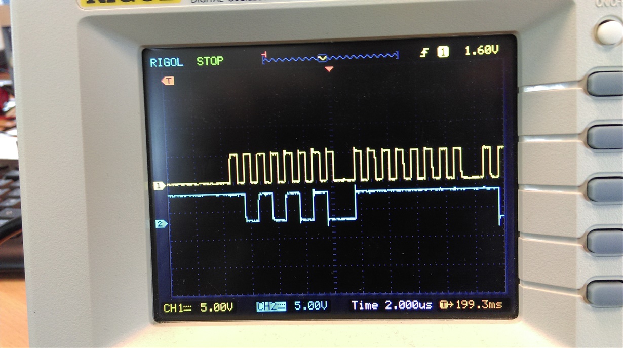
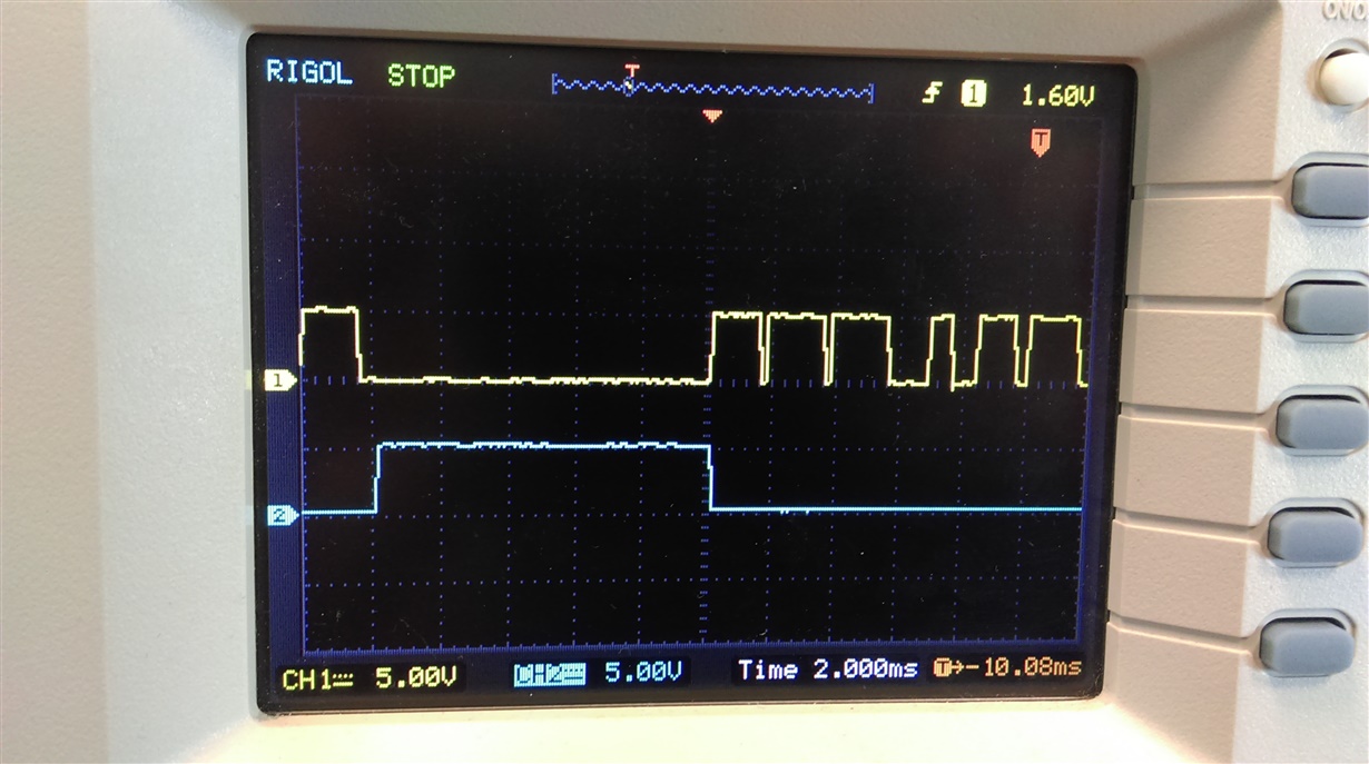
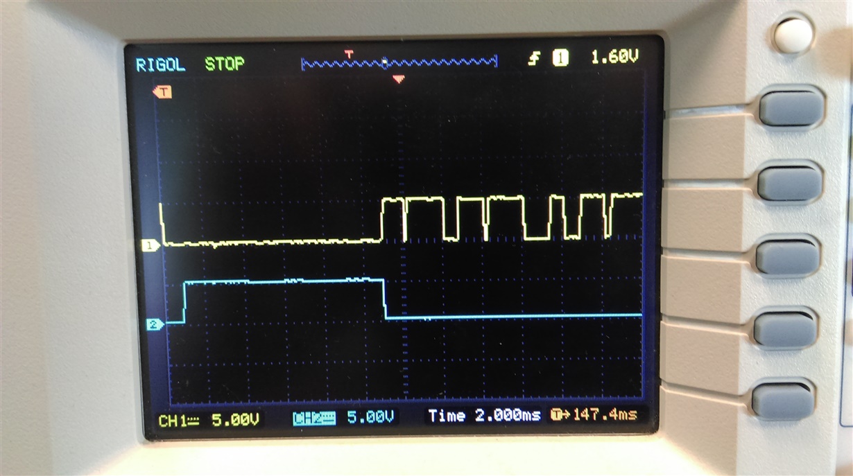
    In the picture below channel 1 (yellow) represents SCK and channel 2 (blue) is MOSI. I have transmitted 0xAA and 0xFF just to illustrate that 0xFF shows a high signal.

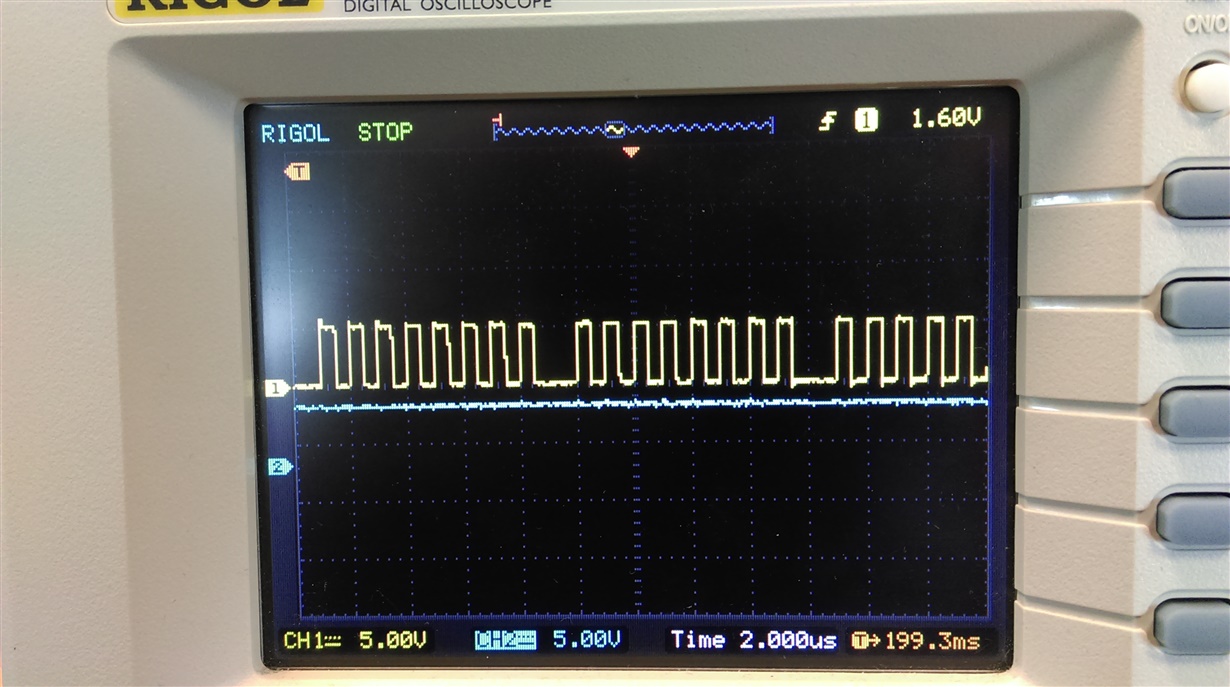
    In the picture below I have transmitted 0xff (as dummy code) to generate the clock tick as discussed before. Is this ok to send this like that??

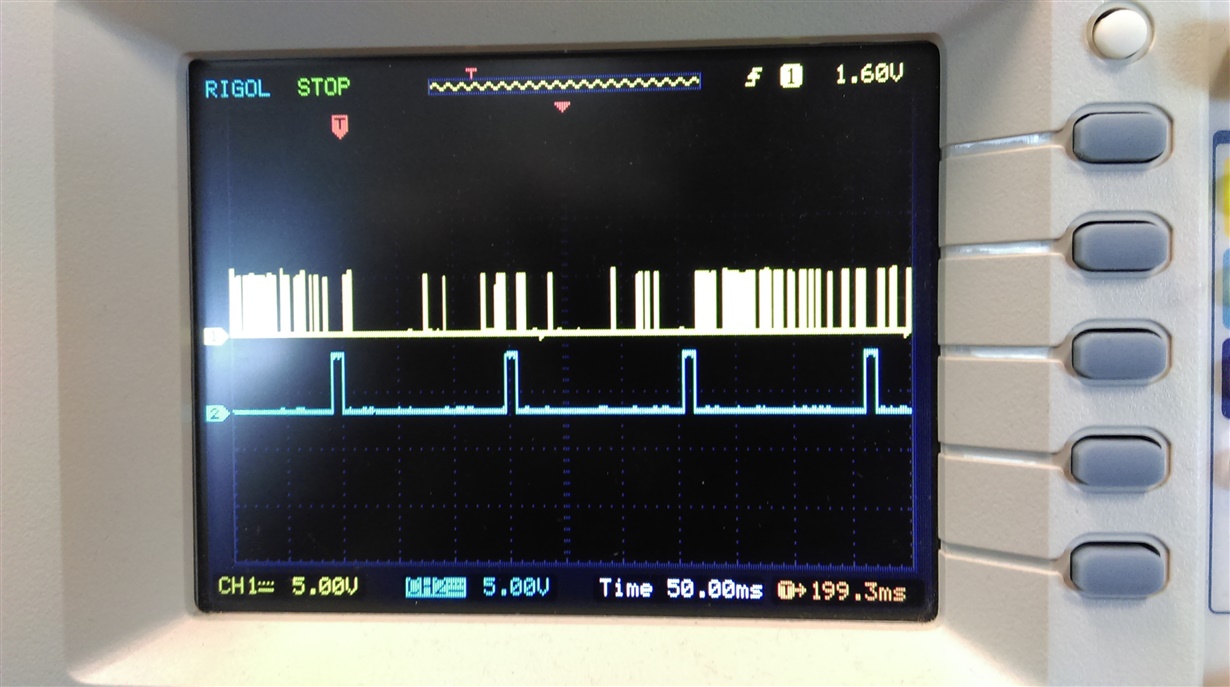
     In the third picture below channel 2 (blue) represents MISO. Notice how the scale has changed from 2 to 50 micro seconds and that a pulse is picked up on MISO every 150uS approx.

    What would be causing this pulse? I am looking to see data that represents a 1Hz square wave.

    Regards,

    Mark.

  • Hey Mark,

    The pulse looks like it lasts about 10ms, but it also looks like it happens to be when there is a gap in your SCLK packets. Is it possible for you to decrease the time per division enough for us to see what is happening on the MISO line right when DRDY falls low and you begin sending SCLKs? I would expect the first 4 bits to be 0xC since that will always begin the status word.

    Regards,
    Brian Pisani
  • Hi again Brian.

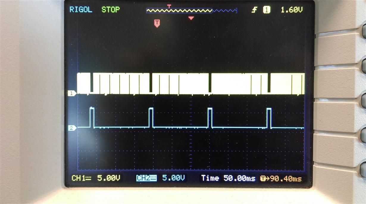
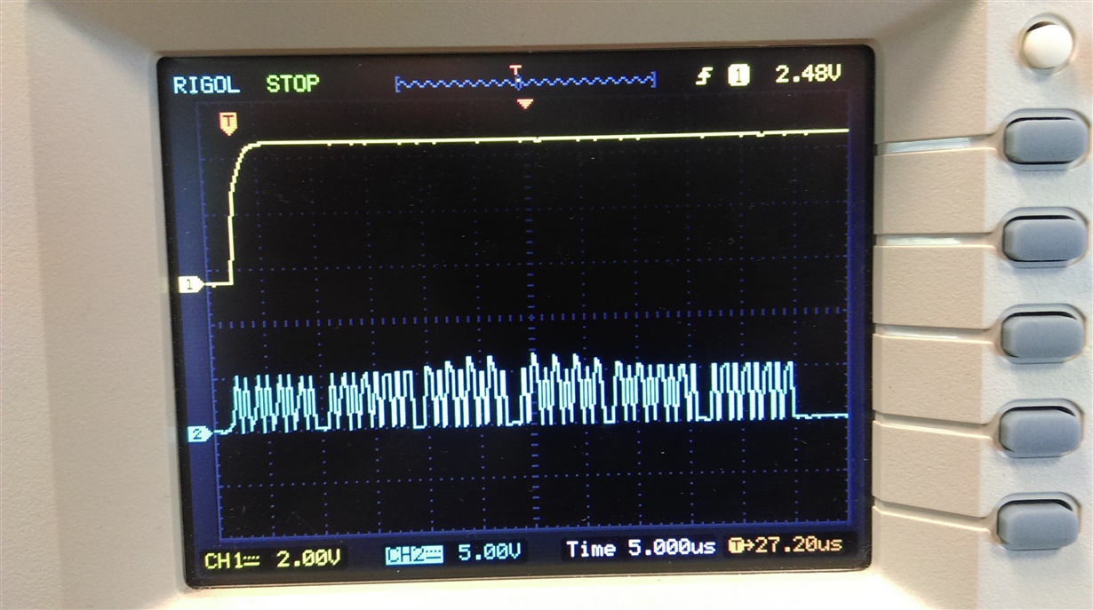
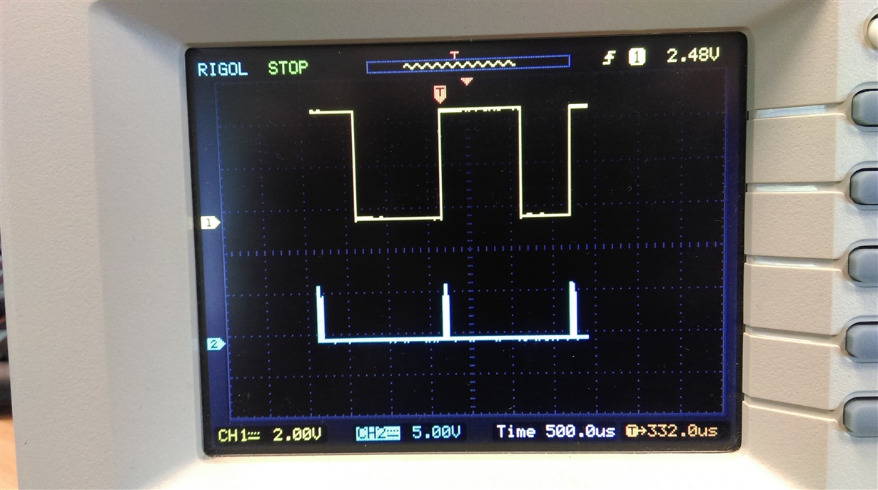
    In the photos channel 1 on top represents the DRDY pin and channel 2 on bottom represents the MISO. The first picture is a zoomed out view  and the other two are zoomed in.

    When DRDY is low You can see a high value on MISO, then DRDY seems to rapidly go on and off. Is this normal as it looks a bit unstable. Surely it should stay low for the duration??

    My pictures are below.

    Thanks again,

    Mark.

    Picture 1.

    Picture 2

    Picture 3

  • Hey Mark,

    The DRDY pin looks like it is behaving how it should when it is in the groupings. The default data rate on the ADS1292R is 500 SPS so the DRDY pin should give a negative edge every (500)^-1 = 2ms. When the DRDYs are grouped together, the negative edges are all 2ms apart. When DRDY is low and never comes high for those intermittent periods of time, are you pulling the START pin low or perhaps the RESET pin? To really see what is going on when the data is exchanged, we need to see what is happening in between the DRDY edges. What we expect to happen is that DRDY falls low then the microcontroller begins to send SCLKs. Once SCLK begins toggling, the DRDY pin will go back high until the next sample. In the mean time, SCLK will toggle enough times to clock all the data out before the next DRDY negative edge. To see the entire transaction that I'm talking about, zoom the scope in so you can see from when DRDY goes low to when the SCLK stops toggling. Given your SCLK frequency (~1 MHz), this should take ~50us so set your scope to approximately 5us/div. From there you should be able to observe everything that happens on a given transaction. I would also recommend reading the SPI interface section of the datasheet thoroughly since it will explain in detail what you should expect to see.

    Regards,
    Brian Pisani
  • Hi Brian.

    The Pics shown seem to agree with what you are saying. I'm deffinately not setting the start and reset pins. I'm at my wits end here going through the code. Config seems to be ok. Is it perhaps the dummy data that I am sending. Is this interfering with the device? What are the usual dummy commands you use??

    Regards,

    Mark.

  • Hey Mark,

    I usually clock in 0x00s when I'm trying to read data out of the device. What is the status of the DOUT pin during the read? With the 5us/div setting you will be able to see the individual bits. Is it always all zeros under this circumstance? I know you are getting zeros back when you read the data on your PC, but as you might imagine that doesn't always mean zeros were transmitted over SPI.

    Brian
  • Hi Brian.

    Something unusual happened. While the program was running i physically reset the chip manually by cutting the power then re powering and then I get data like below. It doesn't resemble a square wave but at least its data.

    Regards,

    Mark.

    127
    255
    255
    192
    0
    0
    127
    255
    255
    192
    0
    0
    68
    211
    149
    192
    0
    0
    127
    255
    255
    192
    0
    0
    127
    255
  • Hey Mark,

    That is real data! The 192-0-0 translates to 0xC00000 in hex which is the 24-bit status byte and as expected it precedes the data points. The 127-255-255 is 0x7FFFFF which is the positive full-scale voltage code for this device. The 68-211-149 corresponds to 0x44D395 which, if you're using the internal 2.42 V reference, corresponds to about 1.3 V. When you reset the device, all register settings will assume their default values so the channels will be converting their pin voltages at startup. To measure the test signal, you have to change the channel register setting. Just so you know, for a +/-1mV square wave, you should expect to see the 24-bit status word 0xCXXXXX followed by a codes that are in the neighborhood of 0x000D8A for +1mV and 0xFFF276 for -1mV (for your system, you'd see decimal byte translations of 0-13-128 for +1mV and 255-242-118 for -1mV). Let me know if you are able to get it to work.

    Brian Pisani
  • Hi Brian.

    Its good that the status byte as expected however the data coming through does not look like as expected. So basically what is happening. I have it configured to generate a square wave. When I run it it all I get is zeros, then I manually reset it by disconnecting and reconnecting the power (not sure why this is, nowhere is it pulled low or reset in code) as this reset sets it back to its default state of data transfer so I should be able to capture the data from the simulator that is connected.

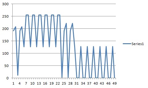
    As there is a 24 bit status byte followed by 24 bits for channel 1 and 24 bits for channel 2 all I am interested in seeing is the middle 3 bytes. For this I am doing 9 SPI transfers to generate the 72 clock tics and just writing the middle 24 to the port. This gives me something that looks like the following:

    Does this look familiar to you? i would expect to see an ECG signal here. The code to generate it is below.

    Regards,

    Mark.


    if((digitalRead(PIN_DRDY)) == LOW)
    {

    digitalWrite(PIN_CS, LOW);

    for(int i=1;i<100;i++){
    Data1 = SPI.transfer(0x00);
    Data2 =SPI.transfer(0x00);
    Data3 =SPI.transfer(0x00);
    Data4 =SPI.transfer(0x00);
    Data5 =SPI.transfer(0x00);
    Data6 = SPI.transfer(0x00);
    Data7 =SPI.transfer(0x00);
    Data8 =SPI.transfer(0x00);
    Data9 = SPI.transfer(0x00);

    Serial.println(Data4);

    Serial.println(Data5);

    Serial.println(Data6);

    }

    Serial.println("Data");

    digitalWrite(PIN_CS, HIGH);
    delay(100);


    }

  • Hey Mark,

    If you cut power to the device, it will power off and all register changes that you made will be lost since the registers are volatile memory. When the device is turned on, the default values will be loaded into the registers. For you to get the be able to see the test signal after you disconnect and reconnect power, you will once again have to write the corresponding values to the channel register.

    The data that you have plotted looks to be byte-length. The data will be the 24-bit concatenation of the data that you collected in Data4, Data5, and Data6 (assuming that you have first configured the channel to convert the test signal). An example of what I mean is below:

    uint32_t data;
    data = (Data4<<16) | (Data5<<8) | (Data6);

    This will produce the valid value for positive voltages, but negative voltages will be in two's complement format, so you'll have to account for the sign in your code.

    Regards,
    Brian Pisani
  • Hi Brian.

    I rewrote the initialisation code so the reset issue is solved. I am still not getting what expected when I re combine the 24 bits. I am getting some very big numbers. What I have been doing is discarding the first and last 24 bits and keeping the middle 24 as they are the ones I am interested in and recombine them as you recommended. Should I discard more or less. You can see from the numbers below that something is not right. The register configuration I have been using is:

    Config1: 0x02
    Config2: 0xa3
    Ch1set: 0x00
    Ch2set: 0x00

    Regards,

    Mark.

    0
    0
    0
    29056
    29056
    29056
    4294934528
    4294934528
    13010
    13010
    13010
    13010
    4294950626
    4294950626
    4294934768
    4294934768
    4294958697
    4294958697
    4294964178
    4294964178
    0
    0
    0
    0
    0
    0
    0
    0
    0
    0
    0
    0
    0
    0
    0
    0
    0
    0
    0
    0
    0
    0
    398
    398
    398
    398
    398
    28631
    28631
    28631
    29139
    29139
    29139
    29139
    31961
    31961
    31961
    31632
    31632
    31632
    1662
    1662
    1662
    1662
    4294967235
    4294967235
    0
    0
    0
    0
    0
    0
    0
    0
  • Hey Mark,

    From you're register settings, it looks like you're enabling the device to generate the test signal, but you do not have the channel configured to measure it. In the CHnSET register page in the datasheet (pg. 43), the final 4 bits configure the input multiplexer for that channel. With your CH1SET register configured as 0x00, you have channel 1 powered on with a PGA gain of 6 measuring the input pins. The results you are seeing are probably the voltage at the input pins, which is not what you are trying to measure. To measure the test signal with channel 1, you must make the lowest 4 bits of the CH1SET register 0101 (0x5) since that corresponds to routing the test signal to the channel.

    To calculate voltage from your conversion results, follow this formula:

    input voltage (V) = [output code*Vref/(2^23 - 1)]/PGA gain

    For your current setup using the internal 2.42 V reference and your channel PGA gain of 6, your calculation would simplify to

    input voltage (V) = output code * 4.81*10^-8

    Regards,
    Brian Pisani
  • Hi Brian.

    That was a typo on my behalf. That should have read.

    Ch1set: 0x05
    Ch2set: 0x05

    Regards,

    Mark.
  • Hi Brian.

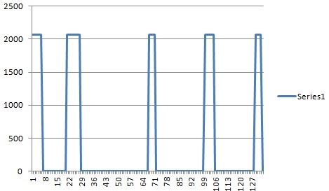
    How accurate is the generated signal. I do have a square wave but its not very periodic.

    Regards,

    Mark.

  • Hey Mark,

    That actually does not look like the correct signal. If you convert the amplitude to voltage, it's only peaking at about 0.1 mV versus the expected 1 mV. Also the signal frequency is supposed to be 1 Hz, which at a datarate of 500 SPS, should correspond to a period of 500 samples. According to the datasheet on page 5, the test signal is accurate within +/-2%. If you set the test signal frequency to DC in the CONFIG2 register, can you measure the DC voltage accurately?

    Brian Pisani
  • Hi Brian.

    I cleaned up the code a bit as there was some redundant pieces causing timing problems. I can see the signal as expected now for both the square wave and dc. I would've assumed that for normal retrieval (using patient stimulator) that the retrieval process would be the same with just the register configurations changed. However I just seem to get very high low values like below. Even with nothing connected I would expect to to see a flat line or some noise.

    The configuration is as follows:

    CONFIG1, 0x02
    CONFIG2, 0xA0
    CH1SET, 0x00
    CH2SET, 0x00

    Is there something I need to add or change??

    Regards,

    Mark.


    0
    0
    2569
    FFFFFFFF
    FFFFFFFF
    FFFFFFFF
    FFFFFFFF
    FFFFAB30
    0
    0
    0
    746C
    FFFFE812
    FFFFFFFF
    FFFFFFFF
    FFFFFFFF
    FFFFFFFF
    6692
    0
    0
    0
    FFFFD930
    4CC1
    FFFFFFFF
    FFFFFFFF
    FFFFFFFF
    FFFFFFFF
    FFFFAA56
    0

  • Hey Mark,

    You're correct; there is no difference in collecting data from the test signal or from the input pins besides what the input mux has the channel connected to. Since your register settings look good then I doubt you're collecting the wrong data. Your data is not actually very large; in contrast, it is very small. I mentioned a few posts ago that the data will be represented in two's complement format. Leading 0xF's in your output data suggest a small magnitude negative number. The data you are receiving looks like an input short condition or something similar. If you're not sure what you should be seeing, you can always try connecting an oscilloscope to the input pins and get a second opinion.

    Regards,
    Brian Pisani
  • Hi Brian.

    I am using one of the following breakout boards:

    www.protocentral.com/.../783-ads1292r-ecgrespiration-breakout-board.html

    with a Rigel 333 patient simulator so fairly sure nothing is shorting. The code below works fine for the test signal but maybe there is something that i am over looking? I have also included some of the data before conversion.

    Thanks again,

    Mark.

    while(1)
    {

    //wait for DRDY==0

    while((digitalRead(PIN_DRDY)) != LOW)
    {
    ;
    }

    digitalWrite(PIN_CS, LOW);


    Data1 = SPI.transfer(0x00);
    Data2 =SPI.transfer(0x00);
    Data3 =SPI.transfer(0x00);
    Data4 =SPI.transfer(0x00);
    Data5 =SPI.transfer(0x00);
    Data6 = SPI.transfer(0x00);
    Data7 =SPI.transfer(0x00);
    Data8 =SPI.transfer(0x00);
    Data9 = SPI.transfer(0x00);


    // digitalWrite(PIN_CS, HIGH);

    datacombined = (Data4<<16) | (Data5<<8) | (Data6);

    voltage = (datacombined * (v_ref / 8388607))/6;

    Serial.println(voltage);


    }

    }


    4294962695
    4294959567
    10889
    4294936625
    4294942419
    28310
    4294962165
    4294940476
    4294943668
    4294934915
    4294942103
    4294956146
    12023
    4294940669
    4294950219
    15983
    4294947877
    4294945900
    4294943787
    4294939406
    4294951118
    4294957993
    11193
    4294940737
    4294937209
    5431
    4294944102
    27133
    18947
    4294961121
    10257
    4294947155
    9675
    4294941701
    4294940028
    4294957532
    24487
  • Hey Mark,

    Your code looks good except that it in its current state it does not account for the negative values in the voltages; but as long as you know while you are debugging that the values will be in two's complement format, then that's ok. I think to check if the conversion is correct, you should connect the scope to the inputs of the ADC and check to see exactly what signal is appearing there.

    Regards,
    Brian Pisani
  • Hi Brian.

    I have tried now using different signal generator with different amplitudes and frequencies and no matter what I do plug it in or out it all looks the same, like noise. When plugged out I would expect to see a flat line, when plugged in I would expect to see peaks but all I see is random data. Do I have to change any other registers for data capture? Is it in the same format : 24 bit status bit, 24 bit for channel one, 24 bit for channel 2? Do I have to change either channel off or on specifically for data capture? Should I process the 32 in some different way??

    Regards,

    Mark. 

  • Hey Mark,

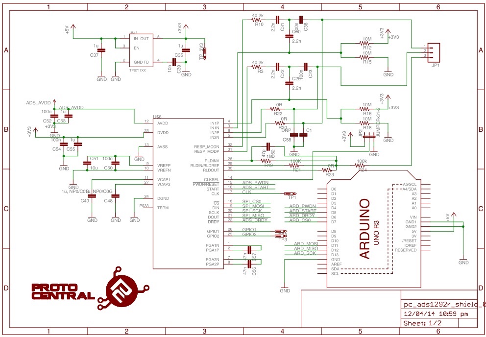
    The output data format will be exactly the same as the case with the test signal. Do you have the respiration modulation and demodulation circuitry enabled for channel 1 inputs? If you do, disable it in the RESP1 register until we get this working. Looking at the schematic for that board, it seems both channel 1 and channel 2 are connected to the board inputs. Is the data you capture the same on channel 2?

    I still believe firmly that this problem could be a hardware issue. Please try probing the signal at the input pins to the ADS1292R. It's important that the probing be done on the device at the input pins so you can tell exactly what signal is reaching the device. If the signal you see there on the scope matches the signal you are generating, we can confidently rule out hardware issues.

    How is your patient simulator generating a common mode voltage for your inputs? Is the RL output from the board being fed to the simulator as a reference input?

    To format the data such that two's complement values are accounted for, I'd recommend just sending the raw unsigned hex values to the PC and decoding them on that side. It will save you some headaches during debug rather than spending significant amount of time just figuring out how the compiler for the microprocessor treats signed versus unsigned integers.

    Regards,
    Brian Pisani
  • Hi Brian.

    The only enabling I have done is:

    CONFIG1, 0x02
    CONFIG2, 0xA0
    CH1SET, 0x00
    CH2SET, 0x00

    Everything else is default.

    The data is the same on both channels. I have probed the signals on both channels and I am seeing what is expected for both between pins 3 - 6. For now I am just using a basic signal generator with 80Hz sine wave @4mV.

    Even with all the noise I would still expect to see some sort of signal. Is it the handling of the samples that may be the problem?? A chuck of the samples are shown below. The consecutive ones looks a bit peculiar. Maybe this has something to do with it.

    Regards,

    Mark.

    11111111111111111001001111111110
    11111111111111111011010111111011
    10000111111001
    11111111111111111100111011110111
    101011110110
    11111111111111111011110111110111
    1000011111001
    11111111111111111001000111111100
    11111111111111111101110011111110
    110101011111111
    10101111111110

  • Hi Brian.

    Something interesting has actually happened. As I was previously been setting my inputs at about 3-5mV it seems that this was too weak and was just getting lost in noise. I was picking up 50Hz mains hum. I have increased my generator to 5 Volts. This was giving me a lot of negative values and looked useless. I have then put an offset of -5 Volts on the generator and I am able to see the signal, works for sine, square and triangular waves. My output is something like the numbers below. I have adjusted my code (below) to read the samples although there is a negative offset. Is it possible to use the millivolt range as the max output from my simulator is 5mV??

    Regards,

    Mark.

    12183
    13936
    15245
    15984
    16010
    15324
    14048
    12298
    10324
    8373
    6783
    5738
    5397
    5873
    7038
    8703
    10638
    12586
    14263
    15456
    16066
    15904
    15084
             uint8_t Data1;
             uint8_t Data2;
             uint8_t Data3;
             uint8_t Data4;
             uint8_t Data5;
             uint8_t Data6;
             uint8_t Data7;
             uint8_t Data8;
             uint8_t Data9;
             
    
             long  datacombined;
             float voltage;
    
     while(1)
     { 
              
              {
              
                      //wait for DRDY==0
                      
                      while((digitalRead(PIN_DRDY)) != LOW)
                      {
                            ;
                      }
                      
                      digitalWrite(PIN_CS, LOW);
    
                      Data1 = SPI.transfer(0x00); 
                      Data2 =SPI.transfer(0x00); 
                      Data3 =SPI.transfer(0x00); 
                      Data4 =SPI.transfer(0x00); 
                      Data5 =SPI.transfer(0x00); 
                      Data6 = SPI.transfer(0x00);
                      Data7 =SPI.transfer(0x00); 
                      Data8 =SPI.transfer(0x00); 
                      Data9 = SPI.transfer(0x00);


                        datacombined = ((((long)Data7<<24) | ((long)Data8<<16) | ((long)Data9<<8)) >> 8);
                        Serial.println( datacombined );
    
                      voltage = datacombined * 0.0000000481;


    }


  • Hey Mark,

    What do those binary words represent? Their length is not uniform.

    Brian
  • Hi Mark,

    It is possible to see them, you just have to filter out the utility noise. You can also increase the PGA gain on the channels to make the signal appear larger in your dynamic range.

    Brian
  • Hi Brian.

    The Binary words are the 32 combined word from the device, " datacombined" When you say their length is not uniform, why? I would expect it to begin at 0 then up to 2^24 representations from the ADC. How should I be seeing these?? For a full min to max signal I would expect to see 0 for min and 16777216 for max. Am I right in saying this?

    As far as filtering goes this is something I will have to do myself. The breakout board was marketed as if ready to plug in and go but I will need to implement some filtering.

    But for the input signal should I be able to input a 3mV signal into the ADS1292R without amplifying it before hand?

    Regards,

    Mark.
  • Hey Mark,

    This device outputs data in two's complement format meaning that the minimum value to expect is the largest negative number you can represent with 24 bits, namely 0x800000. The largest positive value will be 0x7FFFFF.

    Filtering of the utility frequency can be done digitally using a notch filter so you may not need to make radical changes to the hardware.

    You won't need to amplify it beforehand, but you may need to amplify it using the internal PGAs on the ADS1292R.

    Regards,
    Brian Pisani
  • Hi Brian.

    We have being playing around with this for a while and still wont operate as it should. We can generate a perfect test square wave signal which peaks at about +2000 and -2000. This indicates that the device is being read fine and therefore when we inject a test signal and change ChSet back to 0x00 we should be able to see it but to no avail. What I can see and this is quiet weird is that if I set the voltage to 3V and use a -3V dc offset I can capture the waveform. However, I need to use it in the millivolt range with no offset.

    Have you seen this type of problem before? Can I use it in the millivolt range?

    Regards,

    Mark.
  • Hey Mark,

    My theory is that your signal generator is not generating signals in the valid common mode range for the ADC. Have you shorted the grounds between the signal generator and the ADC? What DC voltage are the positive and negative inputs to the channel connected to with respect to each other and respect to AVSS? The individual inputs with respect to AVSS cannot exceed the power supply voltages on either side. The PGA is fully differential so the output of the PGA also may not exceed those limits without clipping. I'd recommend biasing your signal to mid-supply to take advantage of the entire ADC range.

    Regards,
    Brian Pisani
  • I am using the following board so it is not possible to directly short the signal generator to the ADC:

    What DC voltage are the positive and negative inputs to the channel connected to with respect to each other and respect to AVSS? Not sure what you mean by this but from the schematic above I have the signal generator connected to JP1. It is just a standard sine/square wave. I increase the range from the milliVolt up to the Volt range.

     I'd recommend biasing your signal to mid-supply to take advantage of the entire ADC range. This is what I would like to do but at the moment I can only capture a signal with the negative offset which is a bit unusual. 

    Can I connect the way I have described with a standard signal centred on 0 Volts?

    Regards,

    Mark.

  • Hey Mark,

    The "Input Common Mode Range" subsection on page 22 of the datasheet describes the valid input range of the device. Channel 1 on that schematic is already AC coupled which should guarantee that at least the pre-PGA input will be within the proper range. In that case, I would connect the negative output of the signal generator to AVSS and connect the positive output to the positive input to the board. I would give the signal a DC offset of 1.65 V and then send a sinusoid to the device. Check and see if you can see it on channel 1. The negative input will be biased to mid-supply by R12 and R15 so only IN1P will be varying but its common mode will be DC at mid-supply. Make sure respiration is disabled for this scenario (and any time you want to read signal data on channel 1 of the ADS1292R).

    Regards,
    Brian Pisani
  • Hi Mark

    I really need your help, as you did the same thing that i am trying to do and i am also getting 0x00 when reading the first read only register.


    But first i have some basic questions,

    1) Which supply did you use to power up the ADS1292R? because the arduino only have 5v or 3.3v?
    2) did you follow the powerup sequence given in the data sheet to just read the register?
    3) which circuit you used to just read the register? i dont want to read any heart beat, just want to communicate with the chip.
    4) can you send me a code example for arduino, just to read the register?
  • Hello Mark
    I saw your posts regarding ADS1292R communication with Arduino uno,

    I have some basic questions first,
    what power supple did you used to connect the ADS1292R with arduino, as it only have 3.3 and 5v
    and the SPI clock signal is also of 5v rms, is it ok to connect it like this or should i use a level converter?
  • Hi Julia.

    Its been a while since I was working with this and ended up parking it as I had other priorities. I was actually using the following breakout board:

    https://www.protocentral.com/arduino-shields/818-ads1292r-ecgrespiration-shield-v2.html

    This has built in level converters and might make your life a little easier.

    Regards,

    Mark.

  • Hi Mark
    Thanks for the info
    i am unable to buy this product as they are not accepting the orders from Germany, however i have used the same circuit as in this link except the level converters. i already had a level converter and i have attached it to my arduino,

    But all i want to do now is to start this device and read a register so i would know that my SPI communication with the device is working.

    can you help me with this?

    just send me a simple code for arduino where i can read the ID register 0x00
    and print its 8 bit value on serial monitor.
    That would be really helpfull for me
  • Hi Julia.

    You can use the code attached. It is what I was using. You may need to tweak it a bit as I cannot remember what state it was in but it is what I was using to talk to and read from the device.

    Regards,

    Mark.

    #include <SPI.h>
    
    
    String sep = "---------------------------------------------------------";
    boolean debug_msg  = true;
    int n_channels      = 0;
    int blank           = 0;
    
    // pins
    #define PIN_CS  7
    #define PIN_RESET  4
    #define PIN_START  5
    #define PIN_DRDY  6
    #define PIN_LED  13
    
    
    // register commands
    #define READ  0x20
    #define WRITE  0x40
    
    // other
    int gMaxChan = 2;
    int gNumActiveChan = 2;
    int activeSerialPort = 0; //data will be sent to serial port that last sent commands. E.G. bluetooth or USB port
    boolean gActiveChan [2]; // reports whether channels 1..2 are active
    boolean isRDATAC = true;
    
    enum spi_command {
    
                    // system commands
                    WAKEUP = 0x02,
                    STANDBY = 0x04,
                    RESET = 0x06,
                    START = 0x08,
                    STOP = 0x0a,
    
                    // read commands
                    RDATAC = 0x10,
                    SDATAC = 0x11,
                    RDATA = 0x12,
    
                    // register commands
                    RREG = 0x20,
                    WREG = 0x40,
    
    };
     
    enum reg {
    
                    // device settings
                    ID = 0x00,
    
                    // global settings
                    CONFIG1 = 0x01,
                    CONFIG2 = 0x02,
                    LOFF = 0x03,
     
                    // channel specific settings
                    CHnSET = 0X03,
                    CH1SET = CHnSET + 1,
                    CH2SET = CHnSET + 2,
    
                    // lead off status
                    RLD_SENS = 0x06,
                    LOFF_SENS = 0x07,
                    LOFF_STAT = 0x08,
    
                    // other
                    GPIO = 0x0B,
                    RESP1 = 0x09,
                    RESP2 = 0x0A,
    
     
    };
    
    enum ID_bits {
    
                    DEV_ID7 = 0x00,
                    DEV_ID6 = 0x40,
                    DEV_ID5 = 0x20,
                    DEV_ID4 = 0x10,
                    DEV_ID2 = 0x04,
                    DEV_ID1 = 0x02,
                    DEV_ID0 = 0x01,
                    ID_const = 0x10,
                    ID_ADS129x = DEV_ID7,
                    ID_ADS129xR = (DEV_ID7 | DEV_ID6),
                    ID_4CHAN = 0,
                    ID_6CHAN = DEV_ID0,
                    ID_8CHAN = DEV_ID1,
                    ID_ADS1294 = (ID_ADS129x | ID_4CHAN),
                    ID_ADS1296 = (ID_ADS129x | ID_6CHAN),
                    ID_ADS1298 = (ID_ADS129x | ID_8CHAN),
                    ID_ADS1294R = (ID_ADS129xR | ID_4CHAN),
                    ID_ADS1296R = (ID_ADS129xR | ID_6CHAN),
                    ID_ADS1298R = (ID_ADS129xR | ID_8CHAN)
    
    };
    
    enum CONFIG1_bits {
    
                    SINGLE_SHOT = 0x00,
                    BIT6 = 0x00,
                    BIT5 = 0x00,
                    BIT4 = 0x00,
                    BIT3 = 0x00,
                    DR2 = 0x00,
                    DR1 = 0x02,
                    DR0 = 0x00,
                    CONFIG1_const = 0x02,
            //SAMP_125_SPS = CONFIG1_const,
            //SAMP_250_SPS = (CONFIG1_const | DR0),
            SAMP_500_SPS = (CONFIG1_const | DR1),
            //SAMP_1_KSPS = (CONFIG1_const | DR1 | DR0),
            //SAMP_2_KSPS = (CONFIG1_const | DR2),
            //SAMP_4_KSPS = (CONFIG1_const | DR2 | DR0),
            //SAMP_8_KSPS = (CONFIG1_const | DR2 | DR1)
              
    
    };


    enum CONFIG2_bits {
    
                    PDB_LOFF_COMP = 0x00,
                    PDB_REFBUF = 0x20,
                    VREF_4V = 0x00,
                    CLK_EN = 0x08,
                    INT_TEST = 0x00, //amplitude = ±(VREFP – VREFN) / 2400
                    TEST_FREQ = 0x00,
    
                    CONFIG2_const = 0x80,
                    INT_TEST_1HZ = (CONFIG2_const | INT_TEST | TEST_FREQ),
                    INT_TEST_DC = (CONFIG2_const | INT_TEST)
    
    };


    enum LOFF_bits {
    
                    COMP_TH2 = 0x00,
                    COMP_TH1 = 0x00,
                    COMP_TH0 = 0x00,
                    VLEAD_OFF_EN = 0x10,
                    ILEAD_OFF1 = 0x00,
                    ILEAD_OFF0 = 0x00,
                    FLEAD_OFF1 = 0x00,
                    FLEAD_OFF0 = 0x00,
                     LOFF_const = 0x10,
                     COMP_TH_95 = 0x00,
                    COMP_TH_92_5 = COMP_TH0,
                    COMP_TH_90 = COMP_TH1,
                    COMP_TH_87_5 = (COMP_TH1 | COMP_TH0),
                    COMP_TH_85 = COMP_TH2,
                    COMP_TH_80 = (COMP_TH2 | COMP_TH0),
                    COMP_TH_75 = (COMP_TH2 | COMP_TH1),
                    COMP_TH_70 = (COMP_TH2 | COMP_TH1 | COMP_TH0),
    
                    ILEAD_OFF_6nA = 0x00,
                    ILEAD_OFF_12nA = ILEAD_OFF0,
                    ILEAD_OFF_18nA = ILEAD_OFF1,
                    ILEAD_OFF_24nA = (ILEAD_OFF1 | ILEAD_OFF0),
                    FLEAD_OFF_AC = FLEAD_OFF0,
                    FLEAD_OFF_DC = (FLEAD_OFF1 | FLEAD_OFF0)
    
    };
    
    
    enum CHnSET_bits {
    
                    PDn = 0x00,
                    PD_n = 0x00,
                    GAINn2 = 0x00,
                    GAINn1 = 0x00,
                    GAINn0 = 0x00,
                    MUXn2 = 0x00,
                    MUXn1 = 0x00,
                    MUXn0 = 0x00,
                    CHnSET_const = 0x00,
                     GAIN_1X = GAINn0,
                    GAIN_2X = GAINn1,
                    GAIN_3X = (GAINn1 | GAINn0),
                    GAIN_4X = GAINn2,
                    GAIN_6X = 0x00,
                    GAIN_8X = (GAINn2 | GAINn0),
                    GAIN_12X = (GAINn2 | GAINn1),


                    ELECTRODE_INPUT = 0x00,
                    SHORTED = MUXn0,
                    RLD_INPUT = MUXn1,
                    MVDD = (MUXn1 | MUXn0),
                    TEMP = MUXn2,
                    TEST_SIGNAL = (MUXn2 | MUXn0),
                    RLD_DRP = (MUXn2 | MUXn1),
                    RLD_DRN = (MUXn2 | MUXn1 | MUXn0)
    
    };


    enum CH1SET_bits {
    
                    PD_1 = 0x00,
                    GAIN12 = 0x00,
                    GAIN11 = 0x00,
                    GAIN10 = 0x00,
                    MUX12 = 0x00,
                    MUX11 = 0x00,
                    MUX10 = 0x00,
                    CH1SET_const = 0x00
    
    };


    enum CH2SET_bits {
    
                    PD_2 = 0x00,
                    GAIN22 = 0x40,
                    GAIN21 = 0x20,
                    GAIN20 = 0x00,
    
                    MUX22 = 0x00,
                    MUX21 = 0x00,
                    MUX20 = 0x00,
                    CH2SET_const = 0x00
    
    };


    enum RLD_SENSP_bits {
    
                    RLD8P = 0x00,
                    RLD7P = 0x00,
                    RLD6P = 0x00,
                    RLD5P = 0x00,
                    RLD4P = 0x00,
                    RLD3P = 0x00,
                    RLD2P = 0x00,
                    RLD1P = 0x00,
     
                    RLD_SENSP_const = 0x00
    
    };


    enum RLD_SENSN_bits {
    
                    RLD8N = 0x00,
                    RLD7N = 0x00,
                    RLD6N = 0x00,
                    RLD5N = 0x00,
                    RLD4N = 0x00,
                    RLD3N = 0x00,
                    RLD2N = 0x00,
                    RLD1N = 0x00,
    
                    RLD_SENSN_const = 0x00
    
    };


    enum LOFF_SENSP_bits {
    
                    LOFF8P = 0x00,
                    LOFF7P = 0x00,
                    LOFF6P = 0x00,
                    LOFF5P = 0x00,
                    LOFF4P = 0x00,
                    LOFF3P = 0x00,
                    LOFF2P = 0x00,
                    LOFF1P = 0x00,
    
                    LOFF_SENSP_const = 0x00
    
    };


    enum LOFF_SENSN_bits {
    
                    LOFF8N = 0x00,
                    LOFF7N = 0x00,
                    LOFF6N = 0x00,
                    LOFF5N = 0x00,
                    LOFF4N = 0x00,
                    LOFF3N = 0x00,
                    LOFF2N = 0x00,
                    LOFF1N = 0x00,
    
                     LOFF_SENSN_const = 0x00
    
    };


    enum LOFF_FLIP_bits {
    
                    LOFF_FLIP8 = 0x00,
                    LOFF_FLIP7 = 0x00,
                    LOFF_FLIP6 = 0x00,
                    LOFF_FLIP5 = 0x00,
                    LOFF_FLIP4 = 0x00,
                    LOFF_FLIP3 = 0x00,
                    LOFF_FLIP2 = 0x00,
                    LOFF_FLIP1 = 0x00,
     
                    LOFF_FLIP_const = 0x00
    
    };


    enum LOFF_STATP_bits {
    
                    IN8P_OFF = 0x00,
                    IN7P_OFF = 0x00,
                    IN6P_OFF = 0x00,
                    IN5P_OFF = 0x00,
                    IN4P_OFF = 0x00,
                    IN3P_OFF = 0x00,
                    IN2P_OFF = 0x00,
                    IN1P_OFF = 0x00,
    
                    LOFF_STATP_const = 0x00
    
    };


    enum LOFF_STATN_bits {
    
                    IN8N_OFF = 0x00,
                    IN7N_OFF = 0x00,
                    IN6N_OFF = 0x00,
                    IN5N_OFF = 0x00,
                    IN4N_OFF = 0x00,
                    IN3N_OFF = 0x00,
                    IN2N_OFF = 0x00,
                    IN1N_OFF = 0x00,
    
                     LOFF_STATN_const = 0x00
    
    };


    enum GPIO_bits {
    
                    GPIOC2 = 0x00,
                    GPIOC1 = 0x00,
                     GPIOD2 = 0x00,
                    GPIOD1 = 0x00,
                     GPIO_const = 0x0C,
    };
    
     
    enum RESP1_bits {
    
                    RESP_DEMOD_EN1 = 0x80,
                    RESP_MOD_EN1 = 0x40,
                    RESP_PH2 = 0x00,
                    RESP_PH1 = 0x08,
                    RESP_PH0 = 0x00,
                    RESP_CTRL1 = 0x02,
                    RESP_CTRL0 = 0x00,
                     RESP1_const = 0x00,
    
                     RESP_PH_22_5 = 0x00,
                    RESP_PH_45 = RESP_PH0,
                    RESP_PH_67_5 = RESP_PH1,
                    RESP_PH_90 = (RESP_PH1 | RESP_PH0),
                    RESP_PH_112_5 = RESP_PH2,
                    RESP_PH_135 = (RESP_PH2 | RESP_PH0),
                    RESP_PH_157_5 = (RESP_PH2 | RESP_PH1),
     
                    RESP_NONE = 0x00,
                    RESP_EXT = RESP_CTRL0,
                    RESP_INT_SIG_INT = RESP_CTRL1,
                    RESP_INT_SIG_EXT = (RESP_CTRL1 | RESP_CTRL0)
    
    };
    
    enum RESP2_bits {
    
      CALIB_ON = 0x00,
      RESP_FREQ = 0x00,
      RLDREF_INT = 0x02,
      BIT0 = 0x01,
      RESP2_const = 0x02,
    
    };


    // serial api
    
    boolean read_ads_data              = false;
    boolean serial_send_data           = false;
    boolean valid_cmd                  = false;
    
    enum SERIAL_API {
    
                    S_READ_ADS = 0x67,//                                  = 0xBF,                 // read from the ads
                    S_STOP_READ_ADS = 0x73, //   = 0xFD,                 // stop reading freom the ads
                    S_SEND_SERIAL                                = 0xDF,                 // start sending to the serial interface
                    S_STOP_SEND_SERIAL = 0xFB                   // stop streaming to the serial interface
    
    };


    //---------------------------------------------------------------------------------
    
    // functions


    //utilities
    
    #include <stdarg.h>


    String hex_to_char(int hex_in) {
    
                    int precision = 2;
    
                    char tmp[16];
    
                    char format[128];
    
                    sprintf(format, "0x%%.%dX", precision);
    
                    sprintf(tmp, format, hex_in);
    
                    //Serial.print(tmp);
    
                    return(String(tmp));
    
    }


    void write_byte(int reg_addr, int val_hex) {
    
                    //see pages 40,43 of datasheet -
    
                    digitalWrite(PIN_CS, LOW);
    
                    delayMicroseconds(5);
    
                    SPI.transfer(0x40 | reg_addr);
    
                    delayMicroseconds(5);
    
                    SPI.transfer(0x00);          // number of registers to be read/written – 1
    
                    delayMicroseconds(5);
    
                    SPI.transfer(val_hex);
    
            delayMicroseconds(10);
    
                    digitalWrite(PIN_CS, HIGH);


                    if(debug_msg){
    
                                    Serial.println(sep);
    
                                    Serial.print( "sent:\t" + hex_to_char(reg_addr) + "\t" + hex_to_char(val_hex) + "\t" );
    
                                    Serial.println(val_hex, BIN);
    
                    }
    
    }


    int read_byte(int reg_addr){
    
                    int out = 0;
    
                    digitalWrite(PIN_CS, LOW);
    
                    SPI.transfer(0x20 | reg_addr);
    
                    delayMicroseconds(5);
    
                    SPI.transfer(0x00);          // number of registers to be read/written – 1
    
                    delayMicroseconds(5);
    
                    out = SPI.transfer(0x00);
    
            delayMicroseconds(1);
    
                    digitalWrite(PIN_CS, HIGH);


                    if(debug_msg){
    
                                    Serial.println(sep);
    
                                    Serial.println( "sent:\t" + hex_to_char(reg_addr) );
    
                                    Serial.println( "recieved:\t" + hex_to_char(out) );
    
                    }


                    return(out);
    
    }


    void send_command(uint8_t cmd) {
    
                    digitalWrite(PIN_CS, LOW);
    
                    delayMicroseconds(5); // 5 = 6us at 32
    
                    SPI.transfer(cmd);
    
            delayMicroseconds(10);
    
                    digitalWrite(PIN_CS, HIGH);
    
    }


    // initialization


    void init_pins(){
    
            //pinMode(SPICK, OUTPUT);
    
            //pinMode(DIN, INPUT);
    
            //pinMode(DOUT, OUTPUT);
    
                    pinMode(PIN_LED,   OUTPUT);
    
                    pinMode(PIN_CS,    OUTPUT);
    
                    pinMode(PIN_RESET, OUTPUT);
    
                    pinMode(PIN_START, OUTPUT);
    
                    pinMode(PIN_DRDY, INPUT);
    
            digitalWrite(PIN_CS, HIGH);
    
            digitalWrite(PIN_START, LOW);
    
            delay(1);
    
    }


    void init_serial(){
    
                    Serial.begin(115200);
    
                    Serial.flush();
    
                    delayMicroseconds(100);
    
    };


    void init_spi(){


            //SPI.setMOSI(DOUT);
    
            //SPI.setMISO(DIN);
    
            //SPI.setSCK(SPICK);


                    // initializes the SPI bus by setting SCK and MOSI low
    
                    SPI.begin();


                    // spi data mode
    
                    // sets clock polarity and phase
    
                    // CPOL = 0 (clock polarity, clock is idle when low)
    
                    // CPHA = 1 (clock phase , data is shifted in and out on the rising of the data clock signal )
    
                    SPI.setDataMode(SPI_MODE1);


                    // spi clock divider
    
                    // sets relative to the system clock
    
                    // n transitions per cycles (SPI_CLOCK_DIV2 = 1 transition / 2 cycles)
    
                    // DIV4 is arduino default, override to make faster
    
                    // needs to be at least 32, or the clock is too slow, 64 to be safe
    
                    SPI.setClockDivider(SPI_CLOCK_DIV16);


                    // spi bit order
    
                    // sets the order of the bits shifted in and out
    
                    // MSBFIRST = most-significant bit first
    
                    SPI.setBitOrder(MSBFIRST);


                    // Pause
    
                    delay(1);
    
    };


    void init_ads(){
    
                    int chSet;
    
                    // see page 77 for boot sequence


                    // Issue Reset Pulse
    
            digitalWrite(PIN_RESET, HIGH);
    
            delay(1000);
    
            digitalWrite(PIN_RESET, LOW);
    
            delay(1000);
    
            digitalWrite(PIN_RESET, HIGH);
    
            delay(100);


                    // Reset communication
    
            digitalWrite(PIN_CS, LOW);
    
            delay(1000);
    
            digitalWrite(PIN_CS, HIGH);


            // Wait longer for TI chip to start
    
            delay(500);


                    // Send SDATAC Command (Stop Read Data Continuously mode)
    
                    send_command(SDATAC);
    
            delay(10);


            chSet = read_byte(READ | ID);
    
            Serial.print("-- ID" + String(chSet) + "--");


                    // All GPIO set to output 0x0000: (floating CMOS inputs can flicker on and off, creating noise)
    
                    write_byte(GPIO,0x00);


                    if(debug_msg){
    
                                    Serial.println(sep);
    
                                    Serial.println("CONFIGs 1 2");
    
                    }
    
                    write_byte(CONFIG1, SAMP_500_SPS);
    
                    write_byte(CONFIG2, 0xA0);
    
            delay(1000);
    
            //write_byte(CONFIG2, 0xA3); //Actives test signal. Comment this line for normal electrodes


                    if(debug_msg){
    
                                    Serial.println(sep);
    
                                    Serial.println("Check Configs");
    
                    chSet = read_byte(CONFIG1);
    
                    Serial.println("CONFIG1: " + String(chSet) + "\t\t" + hex_to_char(chSet) );
    
                    chSet = read_byte(CONFIG2);
    
                    Serial.println("CONFIG2: " + String(chSet) + "\t\t" + hex_to_char(chSet) );
    
                    }


                    if(debug_msg){
    
                                    Serial.println(sep);
    
                                    Serial.println("Set Channels");
    
                    }
    
                    // Set channels to input signal
    
                    for (int i = 1; i <= gMaxChan; ++i) {
    
                                    write_byte(CHnSET + i, ELECTRODE_INPUT | GAIN_12X);
    
                                    write_byte(CHnSET + i, 0x00); //For test signal 0x05. For normal electrodes 0x00
    
                                    write_byte(CHnSET + i,SHORTED);
    
                    }


                    // Start
    
                    digitalWrite(PIN_START, HIGH);
    
                    delay(150);


                    // get device id


                    //detect active channels
    
                    if(debug_msg){
    
                                    Serial.println(sep);
    
                                    Serial.println("detecting active channels:");
    
                    }
    
                    //gNumActiveChan = 0;


                    for (int i = 1; i <= gMaxChan; i++) {
    
                                    delayMicroseconds(1);
    
                                    chSet = read_byte(CHnSET + i);
    
                                    gActiveChan[i] = ((chSet & 7) != SHORTED);                                                                         // SHORTED = 0x01
    
                                    if ( (chSet & 7) != SHORTED) gNumActiveChan++; 
    
                                    if(debug_msg) Serial.println(String(i) + ": " + String(chSet) + "\t\t" + hex_to_char(chSet) );
    
                    }
    
                    if(debug_msg) Serial.println("detected " + String(gNumActiveChan) + " active channels.");


                    // start reading
    
                    //send_command(RDATAC); // can't read registers when in rdatac mode!


    }


    // get data


    void read_and_send_data(){


                    //Serial.println(sep);


                    //vars
    
                    int numSerialBytes = 1 + (3 * gNumActiveChan); //8-bits header plus 24-bits per ACTIVE channel
    
                    unsigned char serialBytes[numSerialBytes];
    
                    int i = 0;


                    int values[gNumActiveChan];


                    unsigned int a, b, c;


                    // start
    
                    digitalWrite(PIN_CS, LOW);
    
                    delayMicroseconds(1);
    
            //Serial.println("RD");
    
            SPI.transfer(RDATAC);
    
            delayMicroseconds(1);
    
                    // get bytes 1-3
    
                    serialBytes[i++] = SPI.transfer(0x00); // get 1st byte of header
    
            //delayMicroseconds(1);
    
                    SPI.transfer(0x00); //skip 2nd byte of header
    
            //delayMicroseconds(1);
    
                    SPI.transfer(0x00); //skip 3rd byte of header
    
            delayMicroseconds(1);


                    // get channels
    
                    for (int ch = 1; ch <= gMaxChan; ch++) {


                                    a = SPI.transfer(0x00);
    
                    //delayMicroseconds(1);
    
                                    b = SPI.transfer(0x00);
    
                    //delayMicroseconds(1);
    
                                    c = SPI.transfer(0x00);
    
                    //delayMicroseconds(1);


                                    if (gActiveChan[ch]) {
    
                                                    // save 3 bytes per active channel
    
                                                    serialBytes[i++] = a;
    
                                                    serialBytes[i++] = b;
    
                                                    serialBytes[i++] = c;
    
                                    }


                                    if(serial_send_data){ //Here we send the data. Now it only send channel 1 (ch == 1)
    
                                                    //if(ch < gMaxChan){
    
                            if(ch == 1){
    
                                    //Serial.println("-Channel " + String(ch));
    
                                                                    Serial.print( String(a) + " " + String(b) + " " + String(c) + "\n");


                                                    }
    
                                    }
    
                    }


                    // end
    
                    delayMicroseconds(1);
    
            //delay(1);
    
                    digitalWrite(PIN_CS, HIGH);       
    
    }


    void serial_api_get(){


                    // send data only when you receive data:
    
                    if (Serial.available() > 0) {


                                    int serial_in = Serial.read();                                          // read the incoming byte:


                                    // process api
    
                    if(serial_in == S_READ_ADS )                      {read_ads_data = true; valid_cmd = true;Serial.println("start reading --> "); Serial.println(serial_in); Serial.println(" <--");}
    
                                    if(serial_in == S_STOP_READ_ADS )        {read_ads_data = false; valid_cmd = true;Serial.println("stop reading --> "); Serial.println(serial_in); Serial.println(" <--");}
    
                                    if(serial_in == S_SEND_SERIAL )                                {serial_send_data = true;             digitalWrite(PIN_LED, HIGH); valid_cmd = true; }
    
                                    if(serial_in == S_STOP_SEND_SERIAL )    {serial_send_data = false;           digitalWrite(PIN_LED, LOW); valid_cmd = true; }
    
                    else if (valid_cmd == false)            Serial.println("Invalid Command --> "); Serial.println(serial_in); Serial.println(" <--");
    
                    valid_cmd == false;
    
                    }
    
    }


    void serial_api_use(){


                    if(read_ads_data){
    
                                    if (digitalRead(PIN_DRDY) == LOW) {
    
                                                    read_and_send_data();                                                               //only read when data is ready, sending data across serial is in this function!
    
                                    }
    
                    }
    
    };


    // main


    void setup(){


                    // ------------------------------------------------------------
    
                    // init
    
                    delay(1000); 


                    // set pins
    
                    init_pins();


                    // serial
    
                    init_serial();


                    // on!
    
                    if(debug_msg) Serial.println("on");
    
                    digitalWrite(PIN_LED, HIGH);


                    // spi
    
                    init_spi();


                    // ads
    
                    init_ads();


                    // ------------------------------------------------------------
    
                    // do stuff


                    // ------------------------------------------------------------
    
                    // exit


                    // off!
    
                    digitalWrite(PIN_LED, LOW);
    
                    if(debug_msg) Serial.println("off");
    
                    //blinkyblink();


    }


    void loop() {
    
                    serial_api_get();
    
                    serial_api_use();
    
    }