This thread has been locked.

If you have a related question, please click the "Ask a related question" button in the top right corner. The newly created question will be automatically linked to this question.

ADS8881 Missing Codes and Sticky Codes

Other Parts Discussed in Thread: ADS8881, THS4281

Hi,

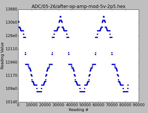
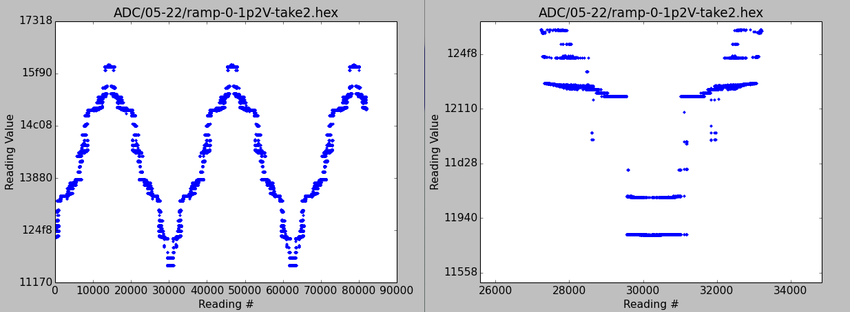
I'm working with the ADS8881 and have been observing what seems to be sticking codes. For the image below, the ADC is reading a 10 Hz triangle wave with Vlow = 2.5V and Vhigh = 3.0V. I've plotted the output in hex. I've looked at the input to the ADC on the oscillosope and it looks like a normal triangle wave with minimal noise.

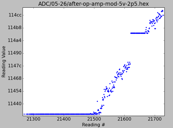
Below is a zoomed-in version. The two "plateaus" are at 0x11430 and 0x114b0.

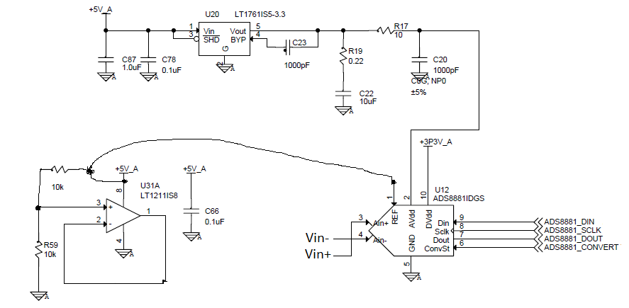
For the test (after-op-amp-mod-5v-2p5) above, the following schematic was used. This is only a partial schematic, so the 5V supply (the output of an LDO) has more bypass caps on it than are shown below.

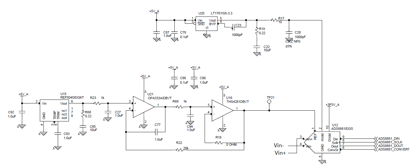
However, when we use a design (see below) very close to a reference design given in the ADS8881 datasheet and give the ADS8881 a 4.5V reference, then the results (also below) look very bizarre.

Here's the corresponding data (same triangle wave input as with the other design), with a section zoomed in at right.

If the input were noisy on the reference were noisy, I'd expect to see a thick fuzzy ramp or random missing codes. Instead, I'm seeing two bands and not much in between.

SPI: 

3-Wire operation Without a Busy Indicator (3-Wire Operation: CONVST Functions as Chip Select)

CONVST = high for 1.0 usec with SCLK = low

length of time between CONVST = low to SCLK = high is 20 nsecs

SCLK =  25 MHZ

  • Not shown is the RC filter on Vin+ and Vin- (R = 10kohm, C = 1nF), as recommended in Fig64 of SBAS547C. SBAS547C is the ADS8881 datasheet.
  • Hi Karen,

    Missing codes and code saturation are typically associated with excessive variation in the reference voltage during the ADC conversion phase.

    A critical component of the reference drive circuit that is missing from your design is the 10uF decoupling capacitor across the output of the THS4281. The closed loop output impedance of the THS4281 increases over frequency and load regulation degrades, causing REF voltage errors whenever there is load current. Installing the bypass cap in parallel with the THS4281 output lowers the output impedance of the circuit at high frequencies. The cap should be placed as close to the ADC as possible to minimize the inductance of the current loop. A small series resistor is also required (about 200mOhm as shown in figure 65 of the datasheet) to ensure that THS4281 buffer provides a stable response as it drives the large cap load.

    Best Regards,

    Harsha

  • Hi Harsha,

    Thanks for your quick response.

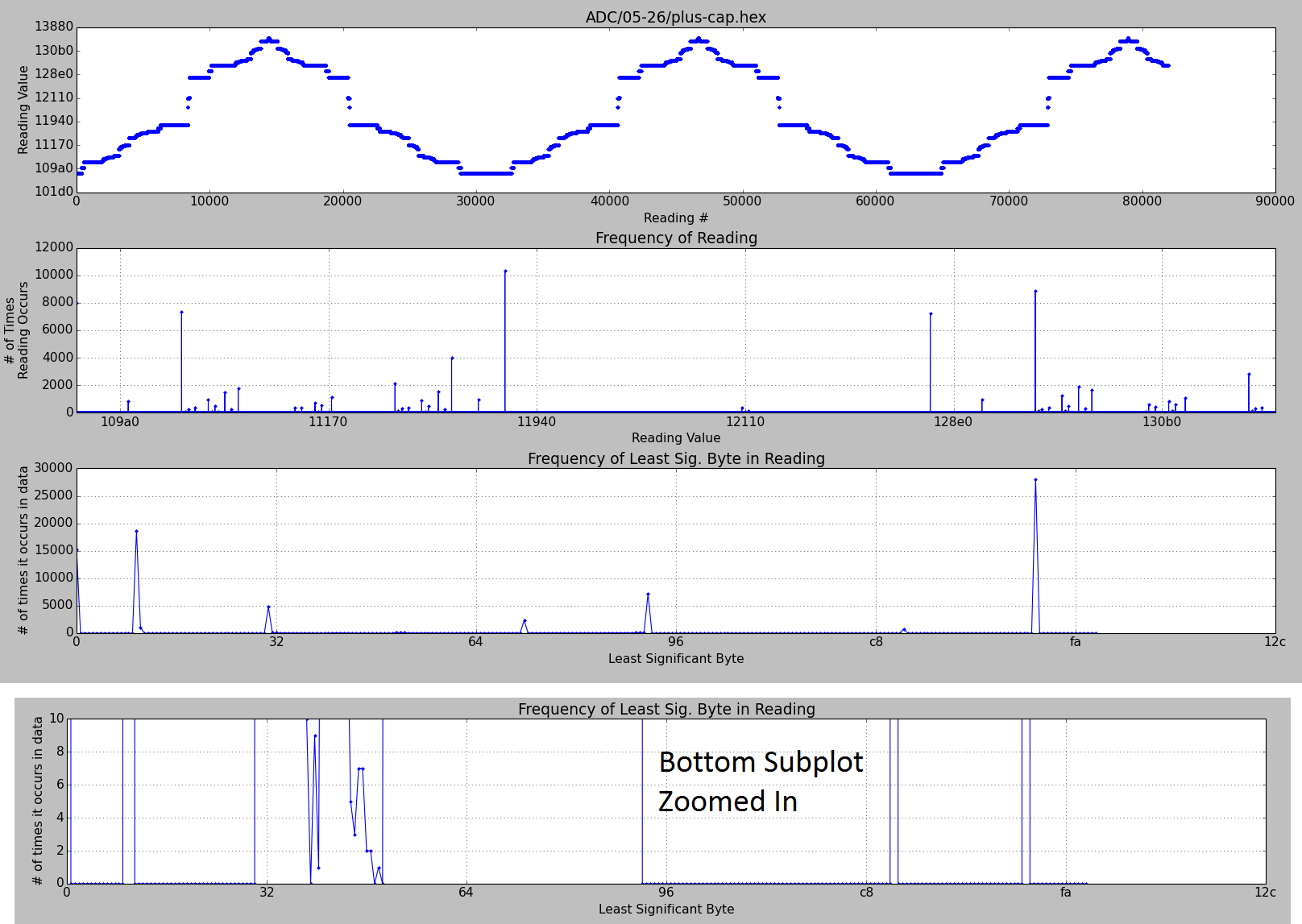
    I've been working with mostly with the first design shown in the beginning of the post, where an op-amp sources the Vref. The plot below is from a test run with that design (after adding the bypass cap). I'll go back to the other design (with the THS4281) and test it with the cap and resistor. Is there a reason to use the THS4281 in particular for Vref, as opposed to a generic op amp?

    I added a 22uF bypass capacitor earlier today (after posting the question) to the REF input on the ADS8881, but didn't see any difference in the output. When I plotted the frequency of the least significant byte of each reading, there were a lot of codes that simply didn't show up in the data. About half of the possible 8-bits values didn't show up in the data, actually. Since it's a triangle wave, we'd expect the frequency of the least significant byte to be uniform. For example, we'd expect to see a reading with LSB 0x80 (e.g. reading = 0x110080) just as often as one with LSB 0x98 (e.g. 0x110098). Even if the voltage reference were changing, I'd expect the least significant bytes to occur at roughly uniform frequency. Do you think there's something going on with the SAR conversion?

  • Hi Karen,

    Driving the REF pin of the ADS8881 requires a wideband op amp to facilitate fast settling of the dynamic REF voltage errors to high accuracy during conversion. To do this we need an op amp that can be used in unity gain configuration to maximize loop gain over frequency, which is required to keep the closed-loop output impedance as low as possible over a wide frequency band. Additionally, since you are powering your op amp buffer off a single +5V supply and the buffer input and output are close to the upper rail, you need an op amp that can support RRIO swing. The THS4281 fits the bill without excessive power consumption and works well in this application.

    The ADC output code distribution for a ramp input is uniform only if the ADC has a linear transfer function. SAR ADC linearity is highly sensitive to extrinsic factors such as the linearity of the input signal source and more importantly, the stability of the reference voltage input.

    I would like to recommend the following experiment to determine whether this is potentially a reference settling issue:

    1) Apply a stable DC voltage to the ADC analog input - short the inputs and connect them to GND for mid-scale input

    2) With the ADC configured for maximum sampling rate perform 10 (or more if you like) back-to-back conversions of the input and record the corresponding ADC output codes

    3) Allow a long delay (a few seconds) for the REF input to settle and repeat steps 2 - 3 multiple times (say 100 sets)

    4) Average each of the 10 samples across the 100 sets to remove noise and plot the 10 samples of the filtered data

    5) You will probably see a gradual settling trend but if the peak to peak difference is several tens of codes then we there is most likely a gross reference settling problem

    Alternatively, you can try driving the REF pin with a battery pack (3*1.5V AA batteries). It would be a good idea to include the 10uF bypass cap close to the ADC.

    Regards,
    Harsha
  • Thanks, Harsha!

    I fly-wired a 10uF capacitor as a bypass cap for the REF pin and that fixed most of the missing codes. The stray inductance from the fly-wiring is probably causing the rest of the missing codes.

  • That is good to hear, Karen :)

    Regards,
    Harsha
  • Hello Karen.

    Can you please clarify something for me, because I am also thinking about my own reference drive circuit and want to understand possible issues: You said earlier that you added a 22µF bypass capacitor to the ref pin and it didn't help, and now you solved the problem by adding a 10µF bypass capacitor. It seems strange that just changing the capacitor value would have such a dramatic effect though, so can you please tell me if there was another crucial difference (e.g. capacitor type, or distance between the cap and the ADC)?
  • Hi Simeon,

    I think the problem was that when I attached the 22uF, I didn't attach it very close to the REF pin on the ADS8881. The flywiring added a lot of extra inductance and the higher ESR of the 22uF might also have had an effect on the filter.

    Cheers,

    Karen

  • Hello Karen,that makes a lot of sense, thank you for clarifying.
    Cheers,
    Simeon