This thread has been locked.

If you have a related question, please click the "Ask a related question" button in the top right corner. The newly created question will be automatically linked to this question.

ADS1278 bit inversion issue

Other Parts Discussed in Thread: ADS1278, CC2530, CC2530EMK


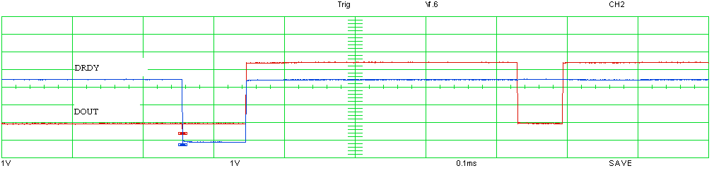
I've interfaced a CC2530 SoC EM with the ADS1278EMK and have written software to acquire readings from the ADS1278 over the SPI interface on USART2 and then forward those readings through the UART on USART1.  I am in SPI-interface mode with TDM dynamic data.  Everything is great with the 1st channel's reading but with the remainder of the channels I get a weird inverted bit issue.

The problem I have is that I am getting an inverted 24bit of the ADC reading at what seems to be randomly.  In other words, a 0x00012D is being read as 0x80012D or a 0xFFF892 as 0x7FF892.  The MSB is the only one that is ever affected with the rest of the bits ok.  Again, this only happens for the channels 2-8, while channel 1 is always read in correctly. 

Is there a requirement that the duty cycle of the SCLK be maintained at 50%? (there is a small lag after each 8 clock cycles because I am using the SPI interface to provide the SCLK with byte transfers).  Do I need use DMA transfers to reduce this lag?  Any other potential issues?


  • RFCE,

    Could you possibly post a screen shot of your SPI transfer?  The MSP430 and CC2530 use an 8-bit clocking scheme, but that should not cause you trouble with the transfer of data.  The serial output is not going to be duty cycle dependent.  I can't think of any reason why you would get an inversion of the MSB unless you are somehow manipulating the B2C output or possibly reading on the wrong clock edge.  However, I should think that would cause trouble with every data set, not just 2-8.

  • It appears that all of the data is shifted by 1 bit.  If I request an additional byte during the read cycle then this last byte will either read 0x00 or 0x80.  In other words, I have to give it (24*number of channels) +1 SCLK cycles to get the full data.  

    From the ADS1278 datasheet, it appears that my SPI settings are correct (negative clock polarity, MSB first, and data input sampled when SCK goes from CPOL inverted to CPOL).  I've tried all other combinations as well and none of them fix this issue.  I have confirmed that at least one CLK cycle occurs between the DRDY and the first SCLK cycle and that the SCLK is at lower frequency than the CLK.  


    Any ideas?

  • OK, so it is clear from the oscilloscope that the DOUT is not being set until DRDY rises back after the first falling edge of the SCLK.  This is inconsistent with the datasheet though.

    What I have done is made sure that the Channel 0 differential voltage is negative so that the MSB should be 1 as a result of the two's complement.  From the scope images below it is clear that the DOUT is not prepared until DRDY rises at the first falling edge of the SCLK.  My understanding is that the MSB of DOUT is supposed to be valid immediately after DRDY falls low.  Is there an error in the datasheet or something else that would cause this behavior?


    SCLK versus DOUT

    DRDY versus DOUT (not aligned with image above)

  •  

    Hi RFCE,

    Sorry for the delay in getting back to you.  We've been going over these screen shots and are wondering what type of scope you are using to capture these images.  Is this from an analog scope or is it a logic analyzer?  If the time scale is correct at .1ms, that would put your SCLK speed in the neighborhood of 16MHz and I would expect to see a little delay from the falling clock edges to the data and DRDY transitions.  I've cropped your two shots together to look at the edges.

    If DOUT is the blue trace in the first picture and red trace in the second, DRDY and DOUT is changing exactly on the falling SCLK.  Usually there is a little delay (18ns typical) with DRDY which would be just about 1 minor division if the time scale is 100ns.  DOUT should also hold for a minimum of 10ns, which is not obvious here and I should think it would be at this zoom level.

    Can you get a screen capture with 4 channels showing the CLK, SCLK, DOUT and DRDY all together?  Can you also possibly send along the ADS1278 portion of your schematic so we can try and reproduce your results in our lab in order to figure out why you need the extra clock cycle?


  • Unfortunately, I am stuck using an old digital storage oscilloscope with only 2 input channels so the screen shots I've posted are probably about the best I can do.  The SCLK was actually set much slower, about 20kHz if I remember correctly.  I am using the ADS1278EMK board which I have wired to a SmartRF04EB with a  CC2530EMK board.  

    At this point, I'm managing to get by through treating the SCLK as a digital I/O pin to provide the first clock cycle and then using the SPI transfers to pull in the data.  Not exactly efficient though so it would be a big help to understand why the extra clock cycle is needed.  Otherwise, I'm finding the ADS1278 to be quite an impressive chip!

  • I may be having a similar issue.  I have an ADS1278 board which I am interfacing to an F28335 experimenter kit.  I have both sizes of channels 1 & 2 tied to ground and expect to see small negative or positive conversion values.  Since twos complement format is used, I thus expect each sample to being with at least 10 ones or 10 zeros.  Excluding the MSB, the intial bits all seem to match.  However, the first bit can be different, from the numerouse (>= 8) bits that are all either 0 or 1.

    Following is a scope trace showing a case where the first bit of 0 does not match the many 1's that follow:

    Additionally I have firmware that read the groups of 48 bits (2 x 24) into circular buffer in groups of 3 16 bit words.  The first word and the first half of the second word are the first channels data.  The last 8 bits of the second word and the third word are the channel two data.  Below is some data captured from code composer.  Bit23's that do not agree with outher start bits are shown in red.

    [0] = 0x0000C000@Data
     [0] = 1111111111111111
     [1] = 1000100100000000
     [2] = 0000000110010000
    [1] =
    0x0000C003@Data
     [0] = 1111111111111111
     [1] = 1001111110000000
     [2] = 0000000110001001
    [2] =
    0x0000C006@Data
     [0] = 1111111111111111
     [1] = 1100111000000000
     [2] = 0000000110010100
    [3] =
    0x0000C009@Data
     [0] = 1111111111111111
     [1] = 1101110000000000
     [2] = 0000000110001001
    [4] =
    0x0000C00C@Data
     [0] = 1111111111111111
     [1] = 1011011000000000
     [2] = 0000001110000100
    [5] =
    0x0000C00F@Data
     [0] = 0111111111111111
     [1] = 1010100110000000
     [2] = 0000011100011111
    [6] =
    0x0000C012@Data
     [0] = 1111111111111111
     [1] = 1110110010000000
     [2] = 0000000100011000
    [7] =
    0x0000C015@Data
     [0] = 1111111111111111
     [1] = 1101001100000000
     [2] = 0000000110110000

    I can believe that giving an extra clock pulse before doing the SPI channel may "fix" this issue.  More specifically, doing so would have kept bit 23 and its neighbors to the right all at the same value. 


    My ADS1278EVM settings are as follows:

    SW11.1 = M0 = Off, SW11.2 = M1 = ON, SW11.3 = F0 = ON, SW11.4 = F1 = ON, SW11.5 = F2 = ON, SW11.6 = CLKDIV = 0FF.

    For SW10, 1 & 2 are on and all other are off.

    NN1, NP1, NN2, NP2 are all grounded, others float.

    Channel switches are all toward ADC1278 chip.

    SW1 set to ON BRD

    TOUT = 7.87 MHZ

    For the F28335, I used the following SPI configuration:

    Note:  Ignore the bit rate comments.  I was back to 4.69 MBPS

    void


    // Reset on, rising edge, 16-bit char bits


    // SpiaRegs.SPICTL.all =0x0004;

    SpiaRegs.SPICTL.all =0x04;


    SpiaRegs.SPIBRR =0x0007;

    // With LOSPCP at default value of 2 and 150 mhz sysclock,


    // Bit rate will be 37.5 E 6/(1 + SPIBRR). Use SPIBRR =31 = 0x1F for


    // test because 4.69 is too high.


    // Gives bit rate of 37.5E6 / 32 = 1.17 mbs

    SpiaRegs.SPICCR.all =0x008F;

    // Relinquish SPI from Reset

    SpiaRegs.SPIPRI.bit.FREE = 1;

    // Set so breakpoints don't disturb xmission

    EDIS;

    }

    Any suggestions would be greatly appreciated.  I am trying to evaluate this part. 


    spi_init()

    {

    EALLOW;

    SpiaRegs.SPICCR.all =0x004F;

    John Sotack

  • John,

    It was a while back that I had this issue and unfortunately I cannot remember with all certainty how I fixed this, but to the best of my memory, I believe that the solution was to backoff a little while from the falling edge of DRDY before pulling in the data.  I have a little snippet of code before I read the data over the SPI where I wait for a couple of CLK cycles.  I am fairly certain that the reason for this backoff was to solve the bit error problem I mentioned in my post.  At least that is a good place for you to start.

    Good luck,

    Matthew

  • Thank you for your reply.  Regarding the suggested hold off after the falling edge of ready; I should be about 7 clock cycles out already.  My master clock (CLK to the ADS1278) is just under 8 mhz and the first SCLK edge appears nears 1 us out.

    There was a post regarding providing an extra clock pulse using GPIO.  The data I get is also consistent with the first bit in the entire data set for all channels being other than channel 1 bit 23.  I might try that as well or perhaps move to a different ADC.

    John

  • John,

    I did provide an extra clock pulse with GPIO for a while before I found the fix and that did work.  I would still give a little more back-off a try unless you have strict timing requirements.  I just have my code count a few pulses of the CLK before requesting data.

    I'd stick it out with the ADS1278 as long as you can ... it really is a really great ADC.  I am unaware of any other ADC offering the same mix of simultaneous sampling, 24-bit resolution, excellent passband and alias rejection, and power consumption.  A little costly for small-quantity development, but in the end well worth it.

    Matthew

  • My problem was that the J5.13 of the ADS1278 evaluation board is not DOUT1 directly but rather is fed through a D flip flop as is indicated on the circuit diagram near the end of the users guide.  On the advice of a TI post, I used DOUT1 from J2.1 which gives an unprocessed signal and my problem was solved.

    Thanks to Tony Calabria for pointing out the D Flip Flop issues and suggesting the J2.1.  Also, thank you to TI in general for providing rapid responses through this forum.  It can be a time saver.

    John

  • John,

    Glad to hear your issues were resolved, we had to implement that D flip flop to correct some timing issues with our EVM-PDK motherboard.

    RFCE,

    I'm curious if your issue is also related to the flip flop. Have you tried using J2.1 to receive the data?

  • Kevin,

    I imagine that the issue I had most have also been caused by the D flip flop.  I remember now that I had troubles when using the development board, but it resolved itself when I designed and fabricated my own circuit with the ADS1278.  I don't think that I ever discovered that it was a flip flop that was causing the issue all along.  Thanks for finding the source!

    Matthew

  • The user guide gave me the impression J5.13 was DOUT1 directly.  If you don't look to the circuit diagram, you are not likely to realize a flip flop is in between.

  • John,

    Agreed. The schematic is also very busy which makes it yet more difficult to notice the presence of the D Flip Flop. We've recently re-designed the ADS1278EVM to resolve schematic readability amongst other issues. We'll see if we can have it addressed for the new revision.

    Thanks to both of you for your feedback and involvement in the community helping each other. It's nice to see non-TI posters helping each other out and the forum living up to it's intentions.

  • Another potential issue to correct:

    On my board, the silk screening for J7 for ANN3/ANP3 seems to electrically correspond to channel 1.  Also ANN4 / ANP4 appears to actually be channel 2.

    John