This thread has been locked.

If you have a related question, please click the "Ask a related question" button in the top right corner. The newly created question will be automatically linked to this question.

ADS1256 stability

Other Parts Discussed in Thread: ADS1256, ADCPRO, ADS1256EVM-PDK, ADS1255, TIPD188

Hi all,

I am using ADS1256 for my application.When i short the ADC input (AIN0 and AIN1) at 1000 SPS I am getting stability of only 17 bits. According to datasheet it should be 19 bits.

My supply is AVDD = +5.0 V , DVDD = +3.3 V and VREF = 1.2 V. What should be the issue for this unstability?

Waiting for yor reply.

  • Dear All,

    One more question i want to ask. I apply 1.0 V input to ADC and use ADC in 18 bit mode. So at 5 SPS I get ADC count 156677 and at 1000 SPS I get 100023 where theoritical count is 107041. Internal buffer is ON.
    Please provide any suggestion.
  • Hi Pooja,

    Regarding your first question, are you performing the noise test on the ADS1256EVM or on your PCB?
    Using the ADS1256EVM configured for a data rate of 1kSPS, I observe the noise-free performance to be close to 19 bits (see the ADCPro screenshot below).

    With the ADC input shorted, the main sources of additional noise are power-supply and PCB layout related.

    The ADS1256EVM's power supply noise may be affected by noise coming from the AC power line. I have noticed that in different locations the EVM noise performance may change. In such cases, using a date rate of 50 or 60 SPS, will allow the digital filter to attenuate more power supply noise. Additionally, you can try to use a DC bench power supply instead of the EVM's wall adapter.

    PCB layout may also contribute to additional ADC noise. If the PCB has poor grounding or if there are inductive traces (traces not routed over their respective ground plane, or splits in the ground plane), then system noise may couple into the ADC and be observed in the output codes.

    For your second question, I don't understand what you mean by "18 bit mode" or how you get "107041" as the ideal code to represent a 1V input signal...

    Assuming VREF = 1.2 V and PGA = 1 V/V, a 1V input signal should have an ideal output code =

    • 1V / LSBsize
    • 1V / (4*Vref / [PGA * 2^24])
    • 1V / (4*1.2V / [1 * 2^24])
    • 1V / (286 nV/code)
    • ideal code = 3495253 (decimal) or 0x355555 (hex)

    How are you applying the 1 V input?

    Best Regards,
    Chris

  • Dear Chris,

    Thank you for your reply. When i applied input of 1.0 V and internal ADC buffer is ON at 1000 SPS ADC code is 3211700 and at 5 SPS code is 5016260 where theoritical should be 3495253. So what should be the reason?

  • Hi Pooja,

    Have you verified that your SPI communication is working properly? If the SPI communication is wrong, than these results are meaningless. Have you tried taking more than one sample to see if you read consistent results?

    A gain error so large could be the result of an unstable reference voltage. What is your 1.2V reference source? Have you checked it on an oscilloscope to ensure it is stable and accurate?

    When you write to the device registers to change the data rate, could you also be modifying any other register settings that could have an effect on the input (i.e. the PGA gain)? This doesn't seem like it is the issue, but it is worth checking becuase changing the data rate should not affect the output result like this.

    What is the common-mode input voltage of your 1V differential signal? If the common-mode voltage is not well defined, it may be out of range and causing erroneous results.

    Also, could you attach a schematic of your circuit?

    Thanks,
    Chris

  • Hi, Chris

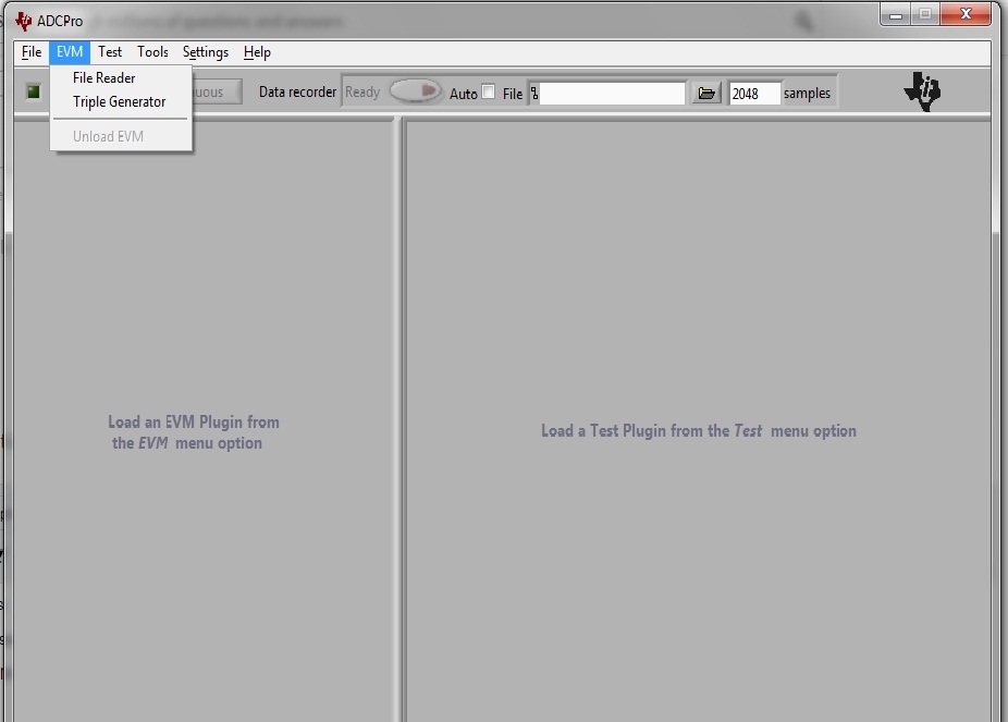
    I purchase ADS1256EVM-PDK and install ADCPro V 2.0.1 but i can not find plugins for ADS1256EVM.

    from EVM dropdown list there is no selection option please find attached image. Please provide path for plugins.

  • Hi Chris,

    above issue is solved it is related to ADS1256 plug-ins.
    One question i want to ask is that in ADCPro software when i set effective data rate to 5.000SPS the channel reading is updated once in a minute. If SPS is 5 reading should be updated 5 times in 1 sec. So what is the reason?
    Is there any averaging on readings? Can I see the reading at 5SPS without any averaging?
  • Hi Pooja,

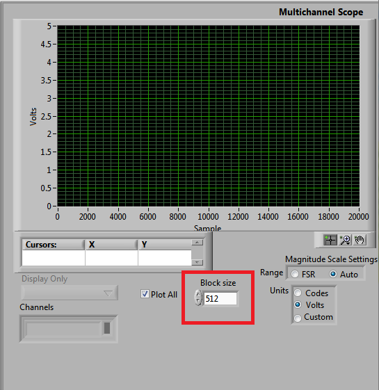
    ADCPro collects data in "blocks", as opposed to streaming data to the PC. By default the block size is 512 samples. Therefore, it takes about  (512 samples / 5 SPS) = 102.4 seconds (plus some overhead) to collect the data.

    You can adjust the block size in the test plug-in:

    Best Regards,
    Chris

  • Hi Chris,

    Thank you for your reply but i want to mak about averaging. Is there a way to see the readings at 5SPS without any averaging on data.
    Also i have noticed one thing that when i set the block size 512 at 5SPS it takes about 102.4 seconds and when block size is 256 it takes almost half time 51 sec but if i reduce the block size to 128 or 64 there is no change in update rate it is same 51 sec.
    What should be the reason? Or is there any other settings for it?
  • Hi Pooja,

    ADCPro does not average or post process the ADC data. When you set the block size to 512 samples, it returns will all 512 samples. You can see the ADC raw data by selecting the "Data Monitor" test plugin.

    There is a minimum block size that ADCPro uses; therefore if you make the block size too small, you won't notice a change in acquisition time. If you don't notice a difference between 128 and 256 samples, then the minimum block size is likely somewhere in that range. For slow data rates, I understand that it can be a little inconvenient to wait for 100's of samples if you are only interested in 10 samples.

    Best Regards,
    Chris

  • Hi Chris,

    Now i want to see the ADC raw data at 5SPS means i want reading to update at every 200msec means 5 SPS per second and for that purpose i require block size 1. So is there any way to check only one reading at 5SPS? Or any other software which allow block size less than 256?

    Please provide suggestion.

  • Hi Pooja,

    I think what your asking for is a way to "stream" data to the PC. Unfortunately, ADCPro does not support data streaming. The intended use case of the ADS1256EVM is to allow for evaluation of the ADC performance. In order to turn the EVM into a data acquisition system, you would need to write your own software.

    ...I'd like to understand  your use case better to help us decide whether to add such a feature to future EVMs. What is your application and how does "data streaming" benefit your use case?

    Thanks and Best Regards,
    Chris

  • Hi Chris,

    Thank you for your reply. ADS1256EVM which i purchased from TI is working OK. And i have created same ADS1256EVM board but i have not mount U4 (256K EEPROM - 24AA256-I/SN) on my board. All other components are same. The issue is that ADCPro can not detect my EVM board it shows error that EVM incompatible.

    What should be the reason? Is EEPROM is necessary to communicate through ADCPro or I can use my board without EEPROM?

  • Hi Pooja,

    ADCPro does check the EEPROM to see if the software is compatible with the EVM hardware. However, you can disable this function by going into C:\Program Files (x86)\ADCPro\plugins\evm\ADS1256\adcpro_evm.ini and changing the 9th line from "EEPROMVerify=TRUE" to "EEPROMVerify=FALSE".

    Best Regards,
    Chris
  • Hi Chris,

    thank you so much your answers are very helpful to me. Please find below my .ini file.

    Name=ADS1256EVM
    PluginType=evm
    FactoryVI=ADS1256EVMFactory.vi
    PanelVI=ADS1256EVMPanel.vi
    Version=2.0.3
    Build=5
    Debug=FALSE
    EEPROMVerify=FALSE

    There is already EEPROMVerify = False but my card is still not working. Is there any other change required to use our board instead of ADS1256EVM?

  • Hi Chris,

    My SPI communication is working properly. I can read ADC registers accurately and at 1000 SPS with Gain 1 i can also get the ADC counts nearly to theoratical count bt as i reduces the SPS my ADC raw count increases.
    What should be the rason? Or is there any timing issue?
    I read the data when i get interrupt at DRDY pin means completes the conversion.
    Please provide suggestion.
  • Hi,

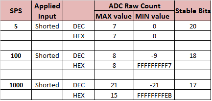
    I am using ADS1256EVM with its modular EVM motherboard itself. I have attached the ADC results at different datarates with input shorted.

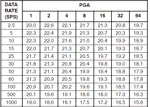
    Where in datasheet of ADS1256 stable bits are as per below table.

    Please provide suggestion.

  • Hi Pooja,

    It sounds like you were able to get ADCPro to connect to your board. I'm not aware of any other requirements, so long as the MMB0 and your board are properly connected. You may need to check the state of the RESET and /PWDN pins on the ADS1256, as well as double check that the correct supply voltages are present).

    As you reduce the ADC data rate, you should see the code counts (i.e. noise) decrease, because the digital filter's noise bandwidth scales with the data rate. The digital filter is similar to a moving average filter that provides additional averaging at the lower data rates.

    Did you say that the opposite behavior was happening; that the noise was increasing for a slower data rate?
    How many samples are you collecting for each data rate? If your sample time increases than it is possible that you input signal is drifting and causing the peak-to-peak code variation to increase as well. However, the input signal should not be drifting if the inputs are shorted and connected to ground.


    I believe you may have posted the same noise table twice. If you could re-post your noise results I'd be glad to look at how they differ from the datasheet noise table.

    Best Regards,
    Chris

  • Hi Chris,

    Sorry for my mistake. Please find table attached below for ADS1256EVM stability with input shorted.

  • Hi Pooja,

    You're getting great results that match the ADS1256 data sheet!

    See below...

    There are a couple things you didn't account for in your calculations...

    1. You're using a 1.2V reference. Therefore, your FSR is only 4*Vref/PGA = 4*1.2/1 = 4.8V.
      In the ADS1256 data sheet a 2.5V reference was used; therefore, FSR was larger (10V for PGA = 1) and Noise-Free Resolution was also higher. You need to subtract about 1 bit of resolution from the ADS1256 data sheet numbers to account for the change in reference voltage.

    2. It seems like you only used a FSR = 2*Vref, when it should be 4*Vref, therefore, you have 1 more bit of resolution.

    See my calculations attached: ADS1256 Noise Calculations.xlsx

    Best Regards,
    Chris

  • Hi Chris,

    I am very thankful to you for your kind support. I am facing one more issue in our ADS1256 board which i previously posted.Please find below.


    My SPI communication is working properly. I can read ADC registers accurately and at 1000 SPS with Gain 1 i can also get the ADC counts nearly to theoratical count bt as i reduces the SPS my ADC raw count increases.
    What should be the reason? Or is there any timing issue?
    I read the data when i get interrupt at DRDY pin means completes the conversion.

    Please find my code below.

    void ADS1255_Update_Reading()
    {
    float temp_val;


    if(ET_ADC_Conversion_Complete == 1)
    {
    ET_ADC_Conversion_Complete = 0;

    adc_raw_count = (float)ADS1255_SPI_READ_Value();

    if(adc_raw_count > 0x3ffff)
    {
    adc_raw_count -= 0x7ffff;
    }

    ReadingL[5] = adc_raw_count;
    temp_val = (float)adc_raw_count * (1.2245 * 2);
    temp_val /= 0x3ffff;
    temp_val /= Gain_divider;
    temp_val *= 100000;

    ReadingL[0] = temp_val;

    }
    }


    void ADS1255_Initialization()
    {

    SSI2_init();

    HWREG(SSI2_BASE + SSI_O_CR0) |= 0x00000080; //Data to be captured on second clock transition

    ROM_GPIOPinTypeGPIOOutput(ADS1255_CS_BASE, ADS1255_CS_PIN);

    ROM_GPIOPinWrite(ADS1255_CS_BASE, ADS1255_CS_PIN, ADS1255_CS_HIGH);
    delay_uSec(100);
    ROM_GPIOPinWrite(ADS1255_CS_BASE, ADS1255_CS_PIN, ADS1255_CS_LOW);
    delay_mSec(2);


    ADS1255_SPI_SEND_Byte(0xFE);
    delay_mSec(2);

    ADS1255_SPI_SEND_Byte(0x50);
    delay_mSec(4);
    ADS1255_SPI_SEND_Byte(0x04);
    delay_mSec(4);
    ADS1255_SPI_SEND_Byte(0xF3); //ADS1255_STATUS
    delay_mSec(4);
    ADS1255_SPI_SEND_Byte(0x01); //ADS1255_MUX
    delay_mSec(4);
    ADS1255_SPI_SEND_Byte(Gain); //ADS1255_ADCON
    delay_mSec(4);
    ADS1255_SPI_SEND_Byte(ADC_SPS); //ADS1255_DATARATE
    delay_mSec(4);
    ADS1255_SPI_SEND_Byte(0xE0); //ADS1255_IO

    delay_mSec(4);

    Reading[0] = (int16_t)ADS1255_Read_Register(ADS1255_STATUS);

    delay_uSec(50);
    Reading[1] = (int16_t)ADS1255_Read_Register(ADS1255_MUX);
    delay_uSec(50);
    Reading[2] = (int16_t)ADS1255_Read_Register(ADS1255_ADCON);
    delay_uSec(50);
    Reading[3] = (int16_t)ADS1255_Read_Register(ADS1255_DATARATE);
    delay_uSec(50);
    Reading[4] = (int16_t)ADS1255_Read_Register(ADS1255_IO);


    ROM_GPIOPinTypeGPIOInput(ADS1255_DRDY_BASE, ADS1255_DRDY_PIN);

    while(ROM_GPIOPinRead(ADS1255_DRDY_BASE, ADS1255_DRDY_PIN) != 0x00);
    ADS1255_SPI_SEND_Byte(ADS1255_READ_DATA_CONT);
    delay_uSec(50);

    ET_ADC_Conversion_Complete = 0;

    GPIOPadConfigSet(ADS1255_DRDY_BASE, ADS1255_DRDY_PIN, GPIO_STRENGTH_8MA, GPIO_PIN_TYPE_STD_WPD);
    ROM_GPIOIntTypeSet(ADS1255_DRDY_BASE, ADS1255_DRDY_PIN, GPIO_LOW_LEVEL);
    ROM_GPIOIntEnable(ADS1255_DRDY_BASE, ADS1255_DRDY_PIN);
    ROM_IntEnable(INT_GPIOD);

    }

    //******************************** Send commands to ADS1255 *******************************
    void ADS1255_SPI_SEND_Byte(unsigned char Data)
    {
    uint32_t Temp_Buffer;

    while(ROM_SSIBusy(SSI2_BASE));
    ROM_SSIDataPut(SSI2_BASE,Data);
    while(ROM_SSIBusy(SSI2_BASE));
    ROM_SSIDataGet(SSI2_BASE, &Temp_Buffer);
    }


    void ADS1255_SPI_Write_Register(unsigned char Address, unsigned char Value)
    {
    Address = (ADS1255_WRITE_REG | Address);

    ADS1255_SPI_SEND_Byte(Address);
    ADS1255_SPI_SEND_Byte(0x00);
    ADS1255_SPI_SEND_Byte(Value);
    }


    unsigned char ADS1255_Read_Register(unsigned char Address)
    {
    uint32_t Buffer[3];
    unsigned char Result = 0;

    Address = (ADS1255_READ_REG | Address);
    ADS1255_SPI_SEND_Byte(Address);
    ADS1255_SPI_SEND_Byte(0x00);

    delay_uSec(50);

    while(ROM_SSIBusy(SSI2_BASE));

    ROM_SSIDataPut(SSI2_BASE, 0xFF);
    while(ROM_SSIBusy(SSI2_BASE));
    ROM_SSIDataGet(SSI2_BASE, &Buffer[0]);

    Result = Buffer[0];
    return Result;

    }

    uint32_t ADS1255_SPI_READ_Value()
    {
    unsigned char i;
    uint32_t Buffer[3];
    uint32_t Result = 0;

    while(ROM_SSIBusy(SSI2_BASE));

    for(i = 0; i < 3; i++)
    {
    ROM_SSIDataPut(SSI2_BASE, 0xFF);
    while(ROM_SSIBusy(SSI2_BASE));
    ROM_SSIDataGet(SSI2_BASE, &Buffer[i]);
    }

    Result = (Buffer[0] << 16) + (Buffer[1] << 8)+ (Buffer[2]);


    Result >>= 5;
    return Result;
    }

    void SSI2_init(void)
    {
    //
    // The SSI2 peripheral must be enabled for use.
    //
    ROM_SysCtlPeripheralEnable(SYSCTL_PERIPH_SSI2);

    //
    // For this example SSI2 is used with PortG[4:7].
    //
    //ROM_SysCtlPeripheralEnable(SYSCTL_PERIPH_GPIOG);

    //
    // Configure the pin muxing for SSI2 functions on port G4, G5, G6, and G7.
    //
    ROM_GPIOPinConfigure(GPIO_PG7_SSI2CLK);
    //ROM_GPIOPinConfigure(GPIO_PG6_SSI0FSS);
    ROM_GPIOPinConfigure(GPIO_PG5_SSI2XDAT0);
    ROM_GPIOPinConfigure(GPIO_PG4_SSI2XDAT1);

    //
    // Configure the GPIO settings for the SSI pins. This function also gives
    // control of these pins to the SSI hardware. Consult the data sheet to
    // see which functions are allocated per pin.
    // The pins are assigned as follows:
    // PA5 - SSI0Tx
    // PA4 - SSI0Rx
    // PA3 - SSI0Fss
    // PA2 - SSI0CLK
    //
    ROM_GPIOPinTypeSSI(GPIO_PORTG_BASE, GPIO_PIN_5 | GPIO_PIN_4 | GPIO_PIN_7);

    //ROM_SSIAdvModeSet(SSI0_BASE, SSI_ADV_MODE_LEGACY);

    //
    // Configure and enable the SSI port for SPI master mode. Use SSI0,
    // system clock supply, idle clock level low and active low clock in
    // freescale SPI mode, master mode, 50MHz SSI frequency, and 8-bit data.
    // For SPI mode, you can set the polarity of the SSI clock when the SSI
    // unit is idle. You can also configure what clock edge you want to
    // capture data on. Please reference the datasheet for more information on
    // the different SPI modes.
    //
    ROM_SSIConfigSetExpClk(SSI2_BASE, ui32SysClock, SSI_FRF_MOTO_MODE_0,
    SSI_MODE_MASTER, 1000000, 8);

    //
    // Enable the SSI0 module.
    //
    ROM_SSIEnable(SSI2_BASE);
    }


    void IntGPIOD(void)
    {
    if(ROM_GPIOIntStatus(GPIO_PORTD_BASE, 1) == ADS1255_DRDY_PIN)
    {
    interrupt_counter++;

    ET_ADC_Conversion_Complete = 1;

    ADS1255_Update_Reading();

    ADS1255_SPI_SEND_Byte(0xFC);
    if(counter_enable > 40)
    counterNo++;
    ROM_GPIOIntClear(ADS1255_DRDY_BASE, ADS1255_DRDY_PIN);
    }
    }

    Please provide suggestion. 

  • Hi Pooja,

    I'm not sure if this part of the code is producing the correct result for you...

    pooja trivedi said:

    adc_raw_count = (float)ADS1255_SPI_READ_Value();

    if(adc_raw_count > 0x3ffff)
    {
    adc_raw_count -= 0x7ffff;
    }

    ReadingL[5] = adc_raw_count;
    temp_val = (float)adc_raw_count * (1.2245 * 2);
    temp_val /= 0x3ffff;
    temp_val /= Gain_divider;
    temp_val *= 100000;

    ReadingL[0] = temp_val;

    The problem is that the ADC code is a SIGNED 24-bit value, but here it is handled as an UNSIGNED 32-bit value and then type-casted to a FLOAT.

    I'd recommend taking the ADC code and sign-extending it into a signed 32-bit data type. Then all you would need to do is multiply by the LSB size (for this operation you'd probably type-cast to a float).

    Best Regards,
    Chris

  • Hi Chris,

    Thank you for your reply. There is no improvement in my ADC results. As i decrease the data rate my ADC count increses. I take the ADC readings when interrupt occurs on DRDY. Is it possible that issue is related to interrupts?
    Can you provide any sample code for ADS156?
  • Hi Chris,

    We are suffering from ADC issues after many weeks. We solve the stability problem but we still stuck at problem of ADC count at different datarate. The issue is from software side so please provide full ADC data read software if possible.
  • Hi Pooja,

    We have ADS1256 example code posted here:

    Additionally, TIPD188 includes a firmware example for a similar device. You can find the download link on the following page:

    It would be good for you to verify the ADC's raw data on an oscilloscope or logic analyzer and verify that it matches what you read in software (look at the raw data, not at the result of the calculations you are performing in software). Once you have confirmed that your software is reading the correct results, then and only then should you debug your calculations to ensure they are being performed correctly in software. Until you've gone through this process, you won't know at what point the invalid data is coming from.

    Best Regards,
    Chris