Hello,
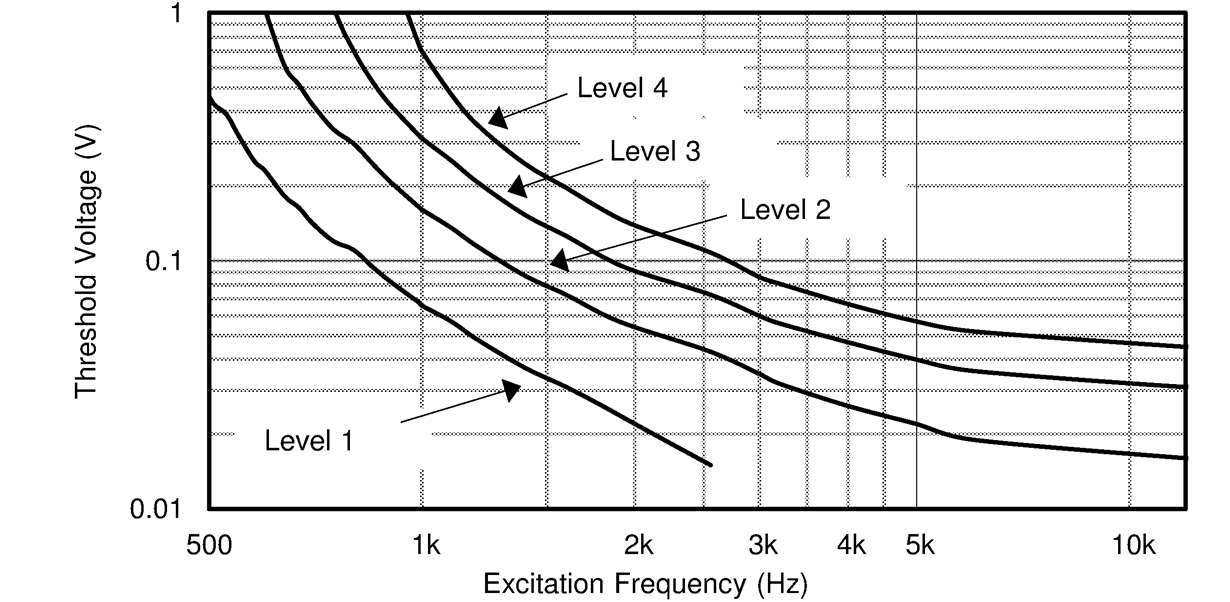
I'm trying to adjust the Analog AC Lead-Off detection with the ADS1293, and I'd like more explanation than what's written in the datasheet. More specifically about the Threshold levels and the way the AC voltage is measured in each input.
I'm configuring the following registers:
LOD_CN 0b00010100 /* Lead Off Detect ON, AC analog, level 1 */
LOD_EN 0b00100000 /* Lead Off Detect ON in IN6 */
LOD_CURRENT 175 /* Lead Off Detect Current is i_lod = 175*8nA = 1,4uA */
LOD_AC_CN 19 /* AC Lead Off Detect frequency: K = 1, ACDIV_LOD = 19 -> freq = 625Hz */
When the datasheet says (8.3.17, page 26):
"The resulting AC current has a frequency Φ and a peak-to-peak amplitude equal to the current programmed into the DAC. An AC coupled synchronous detector detects the amplitude of the AC voltage appearing on the lead. The detected amplitude is compared to a reference voltage by means of a Schmitt-trigger comparator."
My questions are:
1) The detector detects peak amplitude? peak-peak amplitude? or what amplitude measurement of the voltage? I'm asking this because I have to choose the threshold level according to the type of measurement.
2) The peak-peak voltage that should appear on the input IN6 is exactly the product of the peak-peak current set (1,4uA) and the resistance between that input and ground (or some low impedance point such as RLD)? Because I measure exactly twice of the value that I calculate.
3) If the detector detects peak-peak voltage, can it handle a waveform that is not square? I'm asking this because there's an impedance between the input and ground that is not purely resistive. For EMI reduction purposes there is a capacitor from the input to ground, and the waveform gets distorted to a triangle shape.
Thanks,
Gustavo


