This thread has been locked.

If you have a related question, please click the "Ask a related question" button in the top right corner. The newly created question will be automatically linked to this question.

REG: ADS1296 output

Other Parts Discussed in Thread: ADS1296

Hello,

I am using ADS1296 to measure the DC output voltage from the Agilent U8002A single output DC power supply.

I have configured the ADS with the following,

Data rate :- 500 sps

Mode :- High Resolution mode

Gain :- 12

The input voltage was set to 80mV then it was slowly increased from 80mV till 160mV.

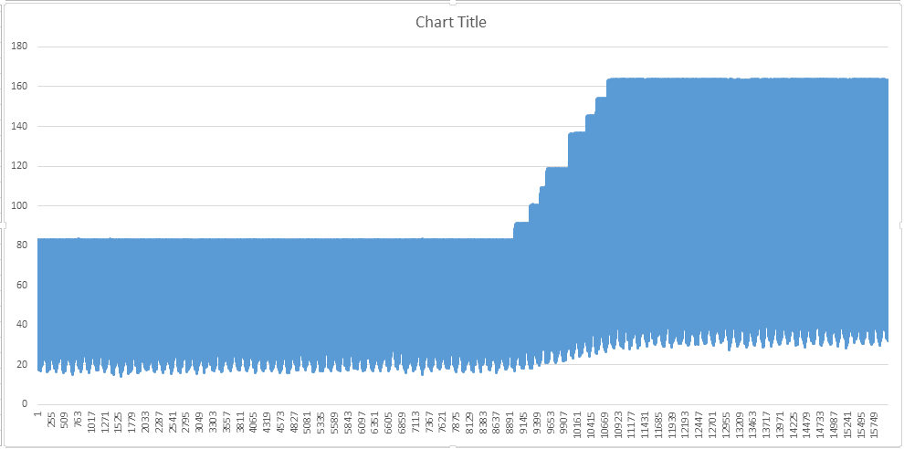
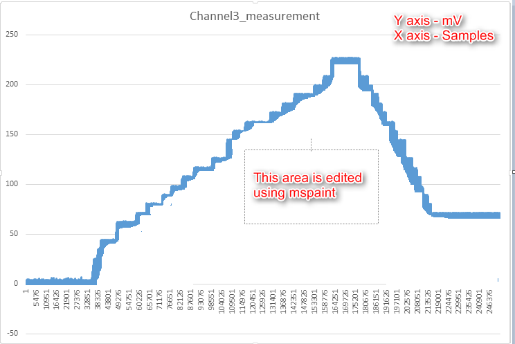
The measured values are then plotted in excel sheet. I was surprised with the plotted values.

I wanted to know why there is a fall in value, instead of the value stays constant?


Please comment.

Thanks,

Nimi

  • Hey Nimi,

    I can't see the picture to copied into the post. Try attaching it by clicking "Use rich formatting" then clicking the paper clip sign in the text editor that comes up. In addition, send me your schematic indicating how the power supply is connected to the inputs.

    Regards,
    Brian Pisani
  • Hello Brian Pisani,

    Thanks for your quick reply.  Sorry for the inconvenience caused.

    Here by I have attached the graph please refer the image,

    Also attached the circuit schematic for your referral,

    SensorBoard.11.pdf

  • Hey Nimi,

    Interesting use for the ADS1296! I would start by probing the inputs to make sure that the signal is getting to the inputs at the voltage you are inputting. I can't tell from the schematic where you are applying the voltage. Are you applying it in lieu of the sensors? I would also be interested to see the hex data of the output. Sometimes spurious output codes can be traced to an interface issue.

    In addition, I am concerned that the external reference being used does not have sufficient bandwidth to meet the switch-capacitor load demands of the reference. If we still cannot identify the problem by ruling out the inputs, I would recommend depopulating the external reference and using the internal reference as a test.

    Regards,
    Brian Pisani
  • Hello Brian Pisani,

    Thanks for the reply.

    Here are the below, which I have tried as per your recommendation.

    1) Removed the 4V external reference from the board,

    2) Enabled the 4V internal reference of the ADS1296 by writing the value 0xE0 in CONFIG3 register.

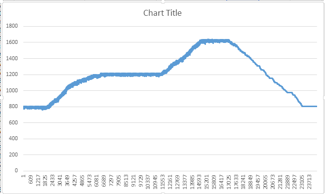
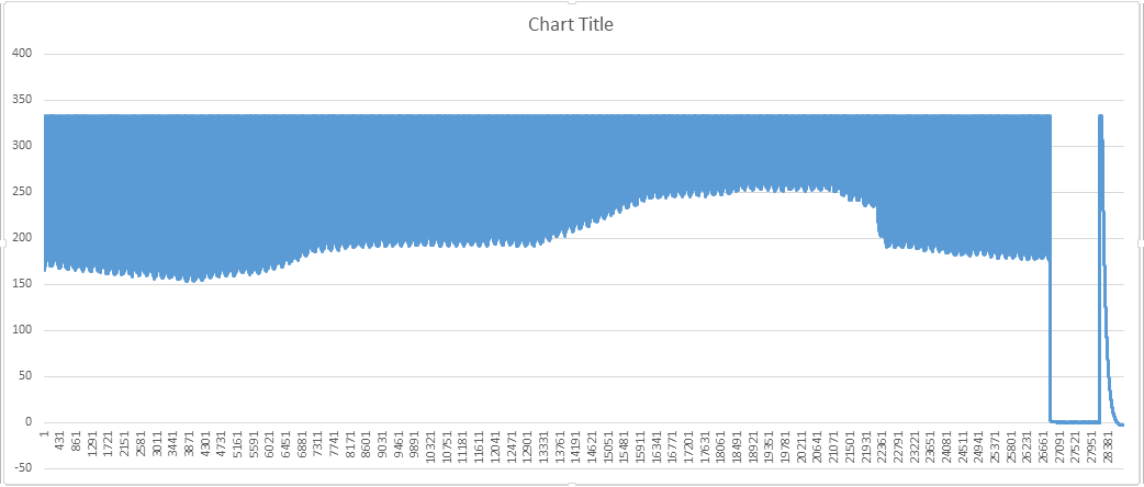
    Now, I have measured the output by changing the input voltage in channel 3 from 80mV to 120mV. I could see the exact output when the gain is set to 1 where as if the gain is set to 12, I am not getting the expected output. Probably my conversion formula used is not right. Here is the conversion formula used,

    reference voltage = 4.0;

    conversion factor  = reference voltage / (2 ^ 23 - 1);

    Output_in_V = { [ channel value ] * (conversion factor) } / gain.

    When Gain == 1,

    When Gain == 12,

    I have also attached the Digital Log for your referral. Please refer Channel 3 for cross verification.ADSlog_gain12.txt

    ADSlog_gain12.txt


    Not able to find why there is a output variation when the gain parameter is the only change from 1 to 12.

    Could you find the problematic area?


    Regards,

    Nimi

  • Hey Nimi,

    The device will output 24-bit two's complement data. Take for example one of your channel 1 data points from your log file : 0xF83146. In decimal, this number corresponds to -511,674. Your conversion factor is correct, and if you multiply this number by the conversion factor, you receive -0.244 V. Dividing by the PGA gain, the voltage at the input comes out to 0.0203. It is difficult to see what either plot is showing. Do your plots correspond to near that voltage and I am not looking at it correctly?
  • Hello Brian Pisani,

    I have connected the input voltage in CHANNEL NO: 3. You may please refer the channel 3`s not the channel 1`s data then you would come to know which is the value I plotted.

    For your information, I have plotted these values in xls sheet. Hope you can also plot the same without any issue.

    BTW, in my previous mail I have highlighted which is the channel number I am referring to.

    Thanks,
    Nimi
  • Hey Nimi,

    Can you post your schematic and your full register settings?

    Brian
  • Hello Brian,

    Please find the attachment for register settings,

    Code used is also attached here,

    ADS1296.c
    void AD1296_init(void)
    {
    	uint8_t data = 0;
    	uint8_t RegData[26];	
    	
    	ADS1296_Data_Stop_Read();
    
    	// Set High resolution mode and  data rate as 8Ksps	
    	data = HIGH_RESOLUTION | DAISY_DISABLE | FMOD_64;	
    	ADS1296_Register_Write(CONFIG1, 1, &data);
    	
    
    	// Enable internal reference
    	data = 0xE0;
    	ADS1296_Register_Write(CONFIG3, 1, &data);
    	
    	// No test signal required
    	data = 0;
    	ADS1296_Register_Write(CONFIG2, 1, &data);
    
    	//Normal input selection
    	data = GAIN_12 | NORMAL_INPUT;
    	ADS1296_Register_Write(CH1SET, 1, &data);
    	ADS1296_Register_Write(CH2SET, 1, &data);
    	ADS1296_Register_Write(CH3SET, 1, &data);
    	ADS1296_Register_Write(CH4SET, 1, &data);
    	ADS1296_Register_Write(CH5SET, 1, &data);
    	ADS1296_Register_Write(CH6SET, 1, &data);
    
    	// Read API call initiated as requested by Brian
    	ADS1296_Register_Read(0x00, 26, RegData);	
    	
    	ADS1296_System_Start_Conversion();
    	
    	ADS1296_Data_Read_Continuous();		
    }
    
    void ADS1296_Register_Write(U8 StartAddress, U8 Count, U8* Data)
    {
    	uint8_t index = 0;
    	
    	// Global array "ADS1296_WriteRegArray"
    	ADS1296_WriteRegArray[0] = WREG | StartAddress;
    	ADS1296_WriteRegArray[1] = Count - 1;
    	
    	for(index = 0; index < Count; index++)
    	{
    		 ADS1296_WriteRegArray[2+index] = Data[index];
    	}
    	
    	// Low level SPI call.
    	spi_master_transfer(ADS1296_WriteRegArray, Count+2, ADS1296_ReadRegArray, Count+2);
    }
    
    void ADS1296_Register_Read(U8 StartAddress, U8 Count, U8* Data)
    {
    	uint8_t index = 0;
    	
    	ADS1296_WriteRegArray[0] = RREG | StartAddress;
    	ADS1296_WriteRegArray[1] = Count - 1;
    	
    	for (index = 0; index < Count; index++)
    	{
    		ADS1296_WriteRegArray[2+index] = 0x00;
    	}
    	
    	spi_master_transfer(ADS1296_WriteRegArray, Count+2, ADS1296_ReadRegArray, Count+2);
    	
    	for (index = 0; index < Count; index++)
    	{
    		Data[index] = ADS1296_ReadRegArray[2+index];
    	}
    }

    Schematic:-

    The input voltage is applied in U798 pin 3 and 4. please find the schematic SensorBoard.pdf

    Question:-

    1) why there is a change in output signal when the gain is changed from 1 to 12. BTW, when gain is 1, I could see the expected output but when the gain is 12, the output is not the expected one.

    Should you require more information, please don`t hesitate to ask.

    Please help me to identify the cause.

  • Hey Nimi,

    First thing I noticed is that the VREF_4V bit is set in the CONFIG3 register. Since you are using an analog power supply of 3.3 V, you will not be able to utilize the 4 V reference ( I should have noticed this previously - my fault!). Clear that bit to use the internal 2.4 V reference and see if your results improve.

    Second, you are using a bench supply to drive the input, correct? If so, what are the voltages with respect to the board AVSS? The device only measures the voltage difference between the two inputs, but the absolute voltage of the inputs themselves must stay within 200 mV of the analog supply rails at a gain of 1. At a gain of 12, this range decreases considerably given that it is the output of the PGA that dictates this range. Hopefully the problem is in one of these two areas.

    Regards,
    Brian Pisani
  • Hello Brian,

    What do you mean by " the absolute voltage of the inputs themselves must stay within 200 mV of the analog supply rails"?

    In which part of the datasheet talks about the above statement? So that I can get some more extra explanation to understand your statement.

    Let me reduce the REF_V to 2.4 and let you know the results.

    Nimi
  • Hey Nimi,

    Refer to equation 2 on page 32. I've seen issues in the past where the inputs were actively driven but they were "floating" with respect to the board supplies. The result is typically strange and unpredictable.

    Brian
  • Hello Brain,

    So for I have not seen the Section 7.3 in page no 12. Analog inputs, the full scale differential input voltage range (AINp-AINn) is ±Vref / gain.

    Now, Vref in my case is 4V and gain is 12V. In that case, the maximum voltage can be measured by ADS is ±333mV.

    Am i correct? Correct me if I am wrong.

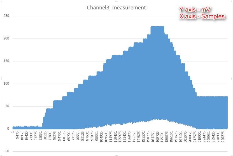
    Now I set the input variation from 0mV to 220mV. I could see the ADS measuring the same. Please find the below,

    Still, the output voltage is not staying constant. Take example at sample 43801 refer graph, i expect the output should stay at 48mV, but it swings between 48mV and zero hence we could see the full area is painted.

    As per my expectation, the graph should be like below,

    But the same behavior is not happening when the gain is 1. Can you find out where the problem could be?

    Regards,

    Nimi

  • Hey Nimi,

    You are correct that if Vref was 4 V and the gain was 12 that your effective input range would be +/-333 mV. A small detail is now you should be using the internal 2.4 V reference since the 4 V reference will not work with AVDD = 3.3V. In that case, your range should only be +/-200 mV, but I digress.

    That rule will determine the voltage that can exist between your positive and negative inputs, but there is another limit which will govern the range of your individual input voltages with respect to the power supplies. Take, for instance, this rather crude but hopefully illustrative example. Imagine you have a voltage of 100 mV which you are trying to measure with the ADS1296. Imagine that, with respect to AVSS, the positive voltage (AINP) is 10.1 V and the negative voltage (AINN) is 10 V. You can see that this AINP-AINN is a 100 mV and 100 mV should be under the differential measurement range for the device. However, it is outside of the supply rails and so connecting it to the inputs of the device would result in an incorrect voltage reading (and in this case you might also damage the device, but that is beside the point). Instead, if you'd like to measure 100 mV, you could instead make AINP = 2.1 V and AINN = 2 V. This will provide a correct reading since the absolute voltages are within the rails of the device. Equation 2 in the datasheet will provide you with the rule for determining correct input ranges by putting things in terms of Vcm, the common-mode input voltage. In the first scenario I proposed, Vcm = 10.05 V, which would violate the rule. In the second example, Vcm = 2.05 V, which is well within the boundary.

    Can you see the distinction I am making between differential input voltage range and common-mode input voltage range? Both requirements must be met in order to get a good conversion. In your case, I am wondering if your voltage source is actively maintained between the board supplies. I am under the impression that the differential voltage that you are trying to convert is "floating" with respect the board supplies and as a result Vcm with respect to AVSS cannot be guaranteed to be within the valid common-mode voltage range. Is this the case?

    Regards,

    Brian Pisani