This thread has been locked.

If you have a related question, please click the "Ask a related question" button in the top right corner. The newly created question will be automatically linked to this question.

AMC7812 thermal pad issue

Other Parts Discussed in Thread: AMC7812

Is it mandatory to use the thermal pad , what happens if it is left  floating for TQFP package??

  • Howdy Akshay and welcome to the E2E forums!

    Each DAC output of the AMC7812 device can supply up to a typical current value of 10mA. If many DAC outputs are providing this sort of current a significant amount of power will be dissipated. The device includes thermal protection in the form of protection circuits that monitor the die temperature. If the die temperature exceeds +150C the alarms will trip.

    Thermal pads help alleviate this accumulation of heat by dispersing it across a plane or large piece of metal, which helps cool the die and prevents it from exceeding the maximum junction temperature value of +150C -- most PCBs include a plane layer (metal layer) underneath the device that the pad connects to through vias.

    If all DAC outputs are in use, with this type of current output then it is highly recommended that the thermal pad be tied to a plane layer, this will help the device stay in spec, and prevent it from exceeding the max junction temp.

    The thermal pad is generally connected to the most negative supply, which in this case is ground (GND).
     
    Matt

  • I have mounted this IC on a small PCB board , in this board there is no provision for this thermal pad connection, so i am leaving it floating , not connected to ground also.
    I will do only small tests and not load the DAC. Hope it works for me.
  • Thanks matthew. It worked for me without grounding the thermal pad.

    How difficult it is to generate a sine wave output from a particular channel using SPI adapter ?

    We have to continously write into device as this is a single register to bring out a sine wave , Delay of 5 micro seconds between successive chip select signals will work?

    Please reply
  • Akshay,

    The DAC update rate is limited by the output voltage settling time as well as the duration of the SPI transaction.  The datasheet reports a typical settling time value of 3us for a 400h to C00h transition.  The SPI transaction is limited by the SCLK frequency.  If you communicate at the fastest SCLK frequency (50MHz), then a complete write will take up approximately 0.48us (24/50e6) -- this assumes CS is pulled high immediately after the last falling edge of SCLK (the minimum time between this transition is 10ns [t7] ).

    Using the information above you can calculate the update rate as 3.48us.

    If you have any other questions please let me know.


    Best Regards,

    Matt

  • Hi Matt

    I was able to generate the sine wave. Thanks for your inputs.

    Now i am seeing a new issue. I am feeding AVCC 5V, AVDD/DVDD 5V, and IOVDD 3.3V. I am programming DAC0 output from 0 to 4095.

    At 0 th code i see 1.2mV , at 1st code again i see 1.2mV, at 2nd code 2.4mV and at 3rd code again 2.4mV. The voltage is changing in pairs.
    For example (0 &1), (2&3) , (4&5) are having same data. Why the data is not changing to 1lsb (1.2mV) wrt each code. What might be the issue?

    Regards
    Akshay
  • Hi Matt

    Please read my issue with respect to 1LSB issue  which i had posted 2 weeks back.

    I have resolved this issue. The issue was with respect to SPI programming.

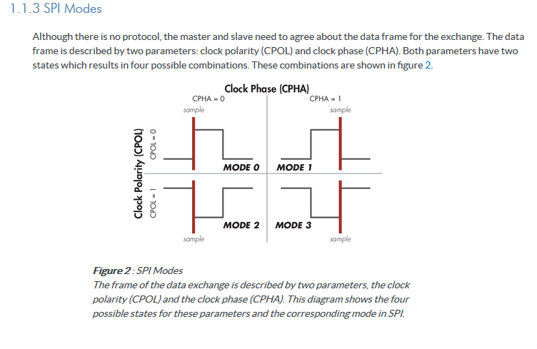
    I was using a cheetah SPI adapter to program the DEVICE , when i was programming using mode0 of SPI adapter the data was changing in pairs. When i changed the mode0 to mode1 , the issue got resolved and 1 LSB change worked fine.

    If you need waveform captures please let me know. Please tell if it is fine to use MODE1 all the time, is this the expected behaviour??

  • Howdy Akshay,


    I'm glad you were able to get it up and running.  Page 12 of the datasheet for the AMC7812 device does display waveforms which are typical to MODE 1 operation.  For instance, Figure 4 of the datasheet shows data captured on the falling edge of SCLK.  SCLK is also shown to start high or low, indicating that correct communication can be achieved through MODE 1 or MODE2.


    Best Regards,

    Matt

  • Hi matthew

    I was trying to see the Glitch and feedthrough impact on my DAC output , but i dont see any glitch and feedthrough on any of the channels.

    Is the DEVICE too good ??? or these are expected on all the devices??

    Regards
    Akshay