This thread has been locked.

If you have a related question, please click the "Ask a related question" button in the top right corner. The newly created question will be automatically linked to this question.

ASD131e04 SPI Speed Vs sampling rate

Other Parts Discussed in Thread: ADS131E04

Hello, 

We are using an ASD131e04 and n the datasheet we have 

tSDECODE Command decode time = 4 tCLKs  ,tCLK = 444 ns, lets say = 4 * 444 = 1776 ns we get a max SPI speed of 563 byte/sec  4,504 MHz ?

if we use 64 Khz we will get 1 data each 15 us ,data frame is 11 bytes, 11 * 8 * 1 / (4,504Mhz ) = 19 us to read the frame with SPI i think i'm missing some thing 

and it seems to me that continous mode should meet the tSDECODE spec also ?

best regards

  • Hello Brahem,

    The decode spec is only for SPI commands. While in RDATAC mode, conversion data will be loaded into the output shift register automatically so it is not necessary to send a command to retrieve data. Simply deassert CS and begin to toggle SCLK after you receive the DRDY signal. The relevant SCLK spec for conversion data retrievals is shown as t_SCLK in Figure 1.

    Regards,
    Brian
  • hello and thank you !
    If I may, i have an other issue, i'm using the ads131e4 to measure voltage from a calibrator with this configuration : 2,4 v reference ,1Khz sampling rate , 5/0V AVDD/AVSS , 3,3V DVDD,IN1P => calibrator output pin, IN1N => calibrator COM pin, and i get this result :
    faultN = 1
    for 1V Input ,data = 1677382
    for 2V Input ,data = 2860514
    i can't send you a picture of the hole schematic

    may be a BIAS voltage is needed??

    Best reagrads

  • Hello Brahem,

    What is the common-mode voltage of your inputs relative to the ADS131E04 supplies? Can you tell me your register settings?

    Brian Pisani
  • Hello these are the registers of the the ads

    Name : ADS131e_Registers[0]
    Decimal:208
    Hex:0xd0
    Binary:11010000

    Name : ADS131e_Registers[1]
    Decimal:150
    Hex:0x96
    Binary:10010110

    Name : ADS131e_Registers[2]
    Decimal:224
    Hex:0xe0
    Binary:11100000

    Name : ADS131e_Registers[3]
    Decimal:197
    Hex:0xc5
    Binary:11000101

    Name : ADS131e_Registers[4]
    Decimal:0
    Hex:0x0
    Binary:0

    Name : ADS131e_Registers[5]
    Decimal:16
    Hex:0x10
    Binary:10000

    Name : ADS131e_Registers[6]
    Decimal:145
    Hex:0x91
    Binary:10010001

    Name : ADS131e_Registers[7]
    Decimal:145
    Hex:0x91
    Binary:10010001

    Name : ADS131e_Registers[8]
    Decimal:145
    Hex:0x91
    Binary:10010001

    Name : ADS131e_Registers[9]
    Decimal:0
    Hex:0x0
    Binary:0

    Name : ADS131e_Registers[10]
    Decimal:0
    Hex:0x0
    Binary:0

    Name : ADS131e_Registers[11]
    Decimal:0
    Hex:0x0
    Binary:0

    Name : ADS131e_Registers[12]
    Decimal:0
    Hex:0x0
    Binary:0

    Name : ADS131e_Registers[13]
    Decimal:0
    Hex:0x0
    Binary:0

    Name : ADS131e_Registers[14]
    Decimal:0
    Hex:0x0
    Binary:0

    Name : ADS131e_Registers[15]
    Decimal:0
    Hex:0x0
    Binary:0

    Name : ADS131e_Registers[16]
    Decimal:0
    Hex:0x0
    Binary:0

    Name : ADS131e_Registers[17]
    Decimal:0
    Hex:0x0
    Binary:0

    Name : ADS131e_Registers[18]
    Decimal:0
    Hex:0x0
    Binary:0

    Name : ADS131e_Registers[19]
    Decimal:1
    Hex:0x1
    Binary:1

    i'm not much of electritian so i suppuse common mode is ((V+) + (V- )/2) witch is 0,5 V??

  • Hey Brahem,

    I meant what is your common-mode voltage with respect to ground the board supplies. The inputs should be biased such that they are within the common-mode input range specified on page 39 of the datasheet.

    Are you able to successfully measure the test signal? Try setting the CH1SET register to 0x15 and look for a 1 Hz square wave.

    Regards,
    Brian Pisani
  • Hello Brian

    no we don't use bias we inject the signal directly to the ADS ,i will try to understand the bias/common-mode stuff and test it/

    For now here are some samples  for the test signals :

    803uV / - 2399806 uV if my calculations are exact 

    2805
    2804
    2811
    2811
    2810
    2809
    2668
    16776547
    16773190
    16773050
    16773050
    16773043

    registers config : 

    Name : ADS131e_Registers[0]
    Hex:0xd0
    Binary:11010000

    Name : ADS131e_Registers[1]
    Hex:0x96
    Binary:10010110

    Name : ADS131e_Registers[2]
    Hex:0xf0
    Binary:11110000

    Name : ADS131e_Registers[3]
    Hex:0xc5
    Binary:11000101

    Name : ADS131e_Registers[4]
    Hex:0x0
    Binary:0

    Name : ADS131e_Registers[5]
    Hex:0x15
    Binary:10101

    Name : ADS131e_Registers[6]
    Hex:0x91
    Binary:10010001

    Name : ADS131e_Registers[7]
    Hex:0x91
    Binary:10010001

    Name : ADS131e_Registers[8]
    Hex:0x91
    Binary:10010001

    other thing with internal ref 4 or 2,4 , I get the same results for example for 1 volt input I get 1669726 from ADS and i can reach 5 v as input and no full scale is detected if i use 5 v as reference in my calculations I get mostly good results (PS : we have 5v connected to the VREFP pin)

  • Hello Brahem,

    Are you applying an external reference while simultaneously powering the internal reference by setting bit 7 of the CONFIG3 register? If that is the case you are creating a short circuit at the REFP pin. You should disable the internal reference if you are using an external reference.

    Regards,
    Brian
  • Hello Brian

    yes we have 5v VREF connected, so basically we can't use internal VREF now?

  • Hello Brahem,

    You cannot use the internal reference buffer while an external reference is connected. The internal reference buffer output voltage comes outside the chip to the REFP and REFN pins for decoupling purposes so if you connect another voltage there, you are creating a short circuit.

    Brian
  • hello Brian !
    thank you for the clarification
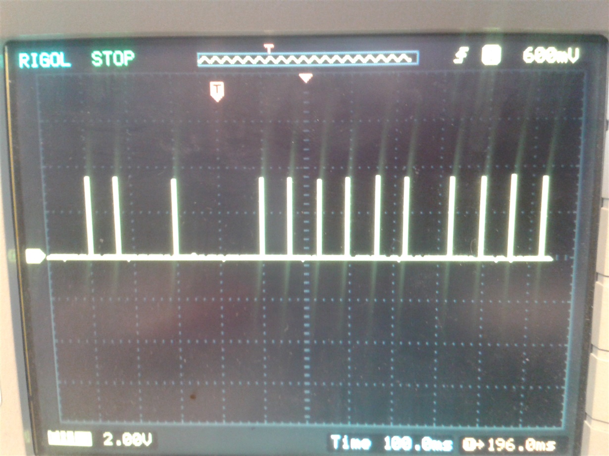
    here is an other issue, we programmed the ADS to work with 1khz sampling rate ,in our code ,we do nothing on the data ready interrupt routine and we got these results (this is the data ready pin)

  • Hey Brahem,

    Are you sure you're not sending SCLKs during this time? DRDY stays high and falls low on a falling SCLK edge.

    Brian
  • Brahem,

    I'm sorry I was mistaken. SCLK causes DRDY to go high. What is the period between the DRDY falling edges when they are closely bunched?

    Brian
  • If you populate another device, is the behavior the same?

    -Brian
  • Would you mind sharing your schematic?
  • I can't send you the whole schematics ,you need something in particular?

  • Hey Brahem,

    I would just like to see connections nearest to the ADS131E04. If you feel more comfortable, you can send it to pa_deltasigma_apps@ti.com and I can review it from there.

    Brian
  • Hello Brian

    I sent the schematics. There is this information, if I read data out from the ADS i get the 1khz with the oscilloscope ,but if not ,I will get a different frequency and strange behavior.

    The microcontroller detects only 2khz speed, which i should figure out why. Any way I need just a clarification for the behavior with no data reading from the ADS ,I need it to debug my code.

    first pic when reading data.

    second we don't read data from ADS.

    thank you

  • Hello Brahem,

    Please try sending it again. The file you sent me was blank. Perhaps try sending it as a PDF to make sure nothing strange happens via email.

    Brian Pisani
  • Hi
    Done .
    other thing the 2Khz problem (I was wrong too it's 500 Hz not 2 Khz) is RTC problem ,so basically if we read data out from ADS every thing is ok
  • Hey Brahem,

    I could not identify anything amiss in the schematic. However I cannot see how the CLK_SEL, RESET, PWDN or CLK pins get configured. Can you describe how each of those work on your board?

    I have a question though. You said that if you read data from the device that the DRDY comes fine and when you do not read then it has problems. How do you know when to read data if DRDY is not functioning properly?

    Regards,
    Brian Pisani
  • for the second question DRDY is always there ,and in the interrupt routine caused by the DRDY if we read data we get DRDY every 1ms we can watch it with the oscilloscope ,but if we don't read data there will be always the DRDY but the timing is wrong.
    for the first question yes the schematic is a little bit messy i'm sorry ,CLK_SEL, RESET, PWDN and CLK are all directly connected to the mcu ,CLK_SEL is set to be internal
  • Hey Brahem,

    Could it be that the scope is not sampling fast enough to catch all the DRDY edges when the device is not retrieving data? It could be that when the device does retrieve data, the "pulse width" of DRDY is wider and the scope could easily capture it.

    Regards,
    Brian Pisani
  • Hello Brian,

    I'm using 2 oscilloscopes with the same results and I can detect DRDY with the mcu and register the timing. I will continue with what have for now i will contact you if I get any new results .

    Thank you :)