This thread has been locked.

If you have a related question, please click the "Ask a related question" button in the top right corner. The newly created question will be automatically linked to this question.

ADS8528 data conversion not stable

Other Parts Discussed in Thread: ADS8528

I am using ADS8528 12 bits ADC. I test it with a 2 volts DC in to the A0. Other voltage levels in to other channels. hardware set to 2XVREF, using parallel interface and hardware set.

I am doing this.

1. Toggle convert pins to high than low, pulse width is about 500 uSec.
2. activate CS#
3. toggle RD# and read data A0, than toggle RD# again to read other channels
4. deactivate CS#

Repeat step 1 to 4 again and loop continues

The data of A0 every time I read is different with huge different and can be +/- 0.7 volts
I checked the DC is good with about 50 mV noise on scope and is stable.
Any hints of what is my problem.
I am behind schedule very much already. Any quick help is appreciated. Thank you.

Rgds

kk chan

  • Hi KK Chan,

    Did you see a BUSY signal out of the ADC? it's a good practice to check the falling edge of BUSY signal, then retrieve the data with /CS and /RD signals to ADC. Can you please upload the schematic including front-end and reference circuit? What's your frequency on CONVST pin? the captured screenshot with scope(CONVST,BUSY,/CS and /RD) will be helpful to address the issue as well. Thanks.

    Regards

    Dale Li

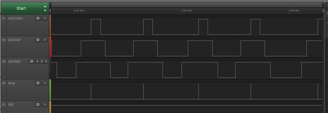
  • Yes. I see BUSY signal. Pulse width is 2 uSec.
    Convert pulse is 250Hz and pulse width is about 500 uSec
    HW#/SW is set to Hardware
    REF/WR# is set to LOW and using external 2.5 volts reference
    Reset is about 4 mSec follow power up
    Range is set to 2XREF
    AB/BA# of 74LVC245A is separated to have individual control line
    1 uF ceramic capacitors are added between pin 55 and 56 and from pin 55 to AGND
    Pull down resistors of 1K ohm are added to both side of 74LVC245A (Interesting, suppose do not need)
    PAR#/SER is set to LOW at parallel mode. Interface is parallel

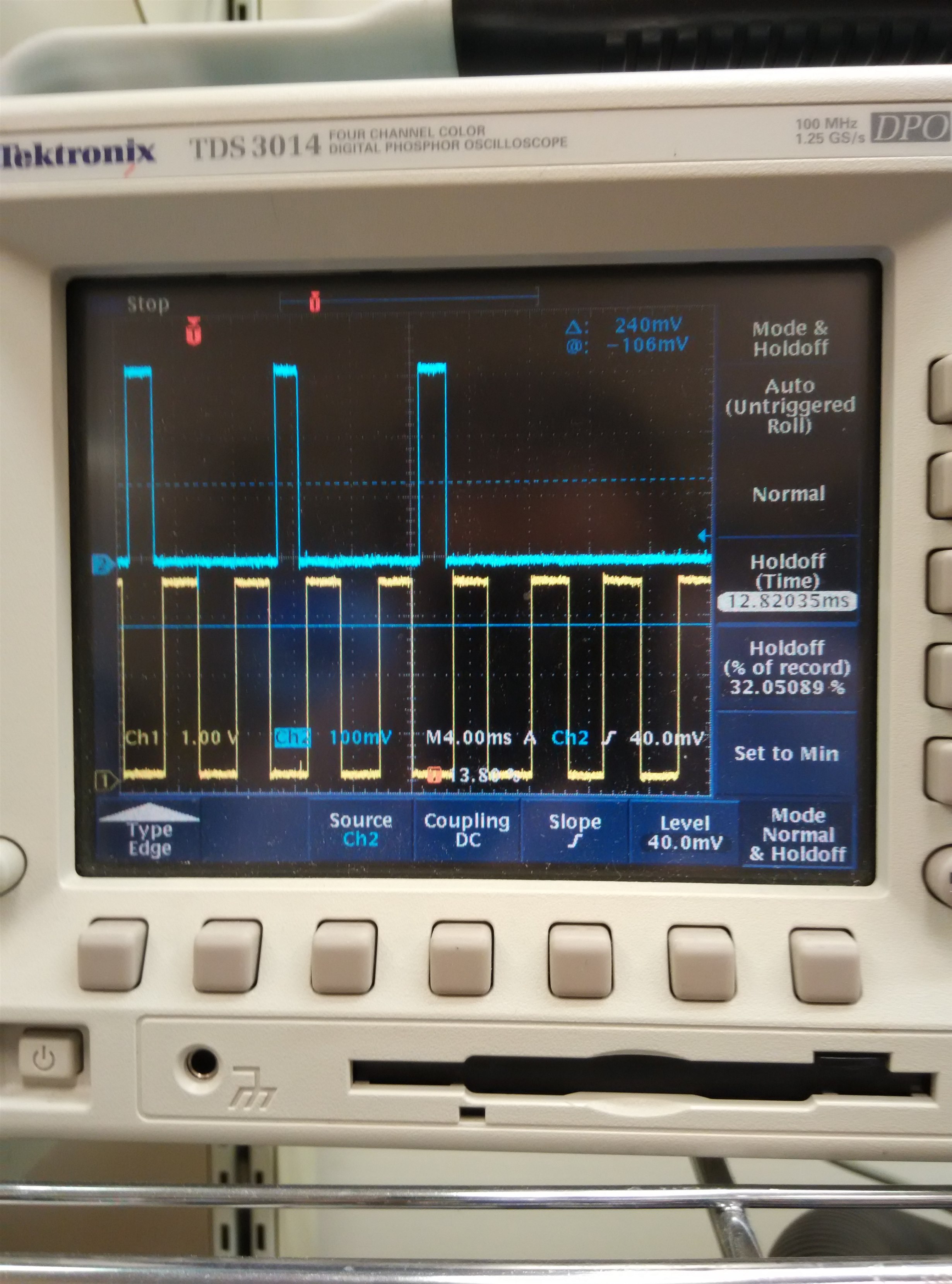
    Attached are schematic, screen capture of logic analyzer and scope for your reference.
    The image captured from the scope is RD# and one data bit

    Any hints? Thank you.

    2626.ADC.pdfADC_Input.pdf

  • Finally, found the stupid mistake.

    The REFN pins are not grounded.

    Thank you very much for you folks help.

  • Hi KK Chan,
    Thank you for your update. Few problems on your hardware circuit:
    1. Yes, REFN(Pin55) should be connected to AGND, also a decoupling capacitor(0.47uF) should be placed between REFIO(Pin56) and REFN(Pin55).
    2. Except above, REFAN(Pin46),REFBN(Pin53),REFCN(Pin60) and REFDN(Pin3) should be connected to AGND.
    3. It's better to have RC filter between external amplifier and ADC, the capacitor can provide the charge to internal sampling capacitor during the acquisition time. Please refer to application example in Figure 45 in datasheet.
    Thanks.

    Regards
    Dale Li