This thread has been locked.

If you have a related question, please click the "Ask a related question" button in the top right corner. The newly created question will be automatically linked to this question.

ADS1274EVM-PDK Malfunction using Function Generator

Other Parts Discussed in Thread: ADCPRO, ADS1278, THS4521, ADS1274

My name is Zachary Trujillo,

I recently purchased the ADS1274EVM-PDK from mouser.com and the product I received seems to be malfunction right out of the box.

The first thing I did was hook up the ADS1274EVM to a function generator.  I used channel 1 with the negative input connected to the internally generated 2.5V which is available at TP3.  This way I could see a signal between 0-5V.  The positive terminal was connected to the output of the function generator.  All jumper and switch settings were verified to be in their default positions.

Waveform was a sine wave with a Vpp of 2V with an offset of 1V, which is well within the range for the ADC.

What was seen on the multiscope of the ADCPro software was the voltage signal just jumping around from +2.5V to -2.5V and only output those two values.  I made sure that Vref in the ADCPro GUI was 2.5V and even verified that the signal from the function generator was correct with an oscilloscope, but I could not get the ADS1274EVM to output the function from the function generator.

I believe the hardware is malfunctioning for this evaluation kit, and I would like to return it to mouser but they informed me that I needed to TI tech support  before that process could be completed.

Thank you in advance for help and guidance.

  • Hi Zachary,

    Thanks for your question.

    To start, could you please share a photo of the EVM as you have it configured? More importantly, this will confirm exactly which version of the EVM hardware you are using.

    If the output in ADCPro is jumping around between +/- 2.5V, then the modulator in the ADS1278 is likely saturating, meaning the differential input voltage is greater than the reference voltage (VREFP - VREFN). I believe TP3 is tied to VREFP, while VREFN is tied to GND. I'm not sure what drive capability the reference source has, but connecting it to the ADC inputs is generally not a good idea without a buffer.

    I would recommend driving your function generator input through the on-board fully-differential amplifiers (FDAs) (should be THS4521 unless you received an out-of-date EVM). These FDAs are great for taking a single-ended input (i.e. 0V - 2V in your case) and converting them to a differential signal with a mid-supply common-mode. The unused input on the FDA can be tied to GND.

    Please share a photo of your EVM setup and we can take it from there.

    Best Regards,

  • Thanks Ryan,

    Sorry for the delayed response I have been a pretty busy student this past couple of days.

    So here is a picture of the EVM setup.  I am using Version F and the FDAs are the THS4521.

    The green jumper cable is going the output of my function generator and the black jumper cable is the ground for the function generator.  I have the FDA buffer enabled for CH1 and i'm using the internally generated VREF.

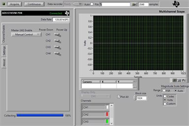
    The function generator is outputting a sine wave with Vpp of 1V with a 0V offset.  Here is the image from the MultiScope of the ADCPro Software:

    This time around I am getting 0V continuously.  I have made sure that my function generator is actually outputting the signal so no problems there haha.

  • Thanks, Zachary.

    TP3 was, in fact, the VREFP input to the ADS1274 (i.e. the ADC voltage reference). Removing the connection between TP3 and the ADC inputs seems to have kept the modulator from saturating.

    The other issue that I see with your setup is that you still have the jumper installed on JP3. This jumper is connected to the /PD ("power-down") pin on the THS4521 amplifiers. Installing this jumper pulls the /PD pins low and disables the input drivers.

    Leave your setup as-is and remove JP3. To verify that the amplifiers are working properly, probe either side of C25 (2.2nF) - keep in mind that you will see half of the differential amplitude.

    Also - remember to share the ground connection between your function generator and the EVM.

    Let me know if this works for you.


    Best Regards,

  • One last thing - Just so that you're aware, there is a known issue with the CLKDIV pin on this version of the EVM (PCB Rev F). It's not the cause of the issue you observed, but some ADC configurations will not be available unless it is corrected. Everything is explained in this errata, which is posted on the EVM product page:

    http://www.ti.com/lit/pdf/slaz645

    To correct the issue, simply cut the trace shown in the picture in this post:

    https://e2e.ti.com/support/data_converters/precision_data_converters/f/73/t/532925

    Best Regards,

  • Okay, so I have removed the JP3 and I still have the buffer selected on CH1.  I connected the ground connection for the function generator to the GND pin at TP4.  I am still getting a 0V output on the MultiScope.  I used the oscilloscope to prove C25 as you suggested, and I can see my signal at half the differential amplitude.

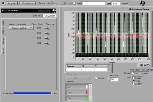
    So I have been trying to figure out why my output is 0V and for some reason I had removed JP13B. So I added it back to the setup and now I am getting the pulses I have seen before.  Here is an image of the MultiScope output.  I still have the negative input to CH1 grounded to AGND from TP1.  I am still using a sine wave with Vpp = 1V and VDC = 0V.

  • Hi Zachary,

    Thanks for the update. Your setup sounds correct to me (with the inclusion of J13B - that's a 5V supply rail used on the daughter board :) ).

    What is the frequency of the sine wave? Can you please share a scope capture of the signal seen at either side of C25? Also, please share a capture of the Settings tab after you've configured the EVM.

    Three more things to try:

    1. See if you can replicate the same issue on all four channels. You can leave them all powered-on in the GUI and provide the inputs through the buffer on each channel, one at a time (remember to move S4, S5, S7 to the right when you do).

    2. Probe the reference voltage across C7. It should be 2.5V.

    3. Make the trace cut outlined in the Errata. I still don't believe it's related to this issue, but it won't hurt to try it and rule it out.

    Please let me know if you are still unable to get the EVM working.

    Best Regards,
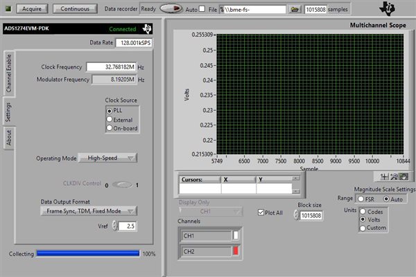
  • The frequency of the sine wave is 1kHz.  Here is a picture of the scope capture across C25 and the image of the settings tab for the EVM.

    Settings Tab:

    Scope Capture of Sine Wave across C25:

    Displaying IMG_2452.JPG

    So I have cut the trace as outlined in a previous discussion link/Errata sheet. I Verified that the trace was with a microscope view and continuity check with multimeter.

    I measured the reference voltage across C7 and it was indeed 2.5V.

    I also switched between CH1-4 with the same output from the function generator.  I made sure to switch on the buffers for each channel.  What was strange is that for channels 2-4 I just got a 0V signal, but for CH1 I got the signal that was imaged in my latest response.  To make sure I was inputting the proper signal to the channels I used the oscilloscope to measure the signal across C23 for CH2, C18 for CH3, and C16 for CH4.  I got the same scope capture as imaged above for all 3 capacitors.

  • Hi Zachary,

    Sorry my delay - I was out of the office for most of last week. Did you have any luck with this issue? It looks like the scope image did not upload correctly, but if you say it was a sine wave, I'll believe you. :)

    If it's alright with you, I'll contact you offline using the email address in your profile.

    Regards,