This thread has been locked.

If you have a related question, please click the "Ask a related question" button in the top right corner. The newly created question will be automatically linked to this question.

Negative Voltage Spikes on DAC8871 output

Other Parts Discussed in Thread: DAC8871, OPA4277

Hi,

I test DAC8871 through SPI Interface @ 50M for an entire dynamic range of +10V to -10V.

As such the output follows the input digital code [driven by an FPGA].

But For digital code equivalent to 0V [8000] and +640mV and +1.25V , I find negative going voltage spikes [so much so from -500mV upto -2.5V.

Why it can be so? Can the timing failure of SPI be code selective or is it some other issue inherent to DAC?

Please help.

  • Hello,

    I am having some difficulties understanding exactly what is happening. Could you perhaps share oscilloscope captures of the SPI inputs that create these issues as well as captures of the behavior of the voltage output itself? A schematic would also be helpful.
  • Hi Kevin,

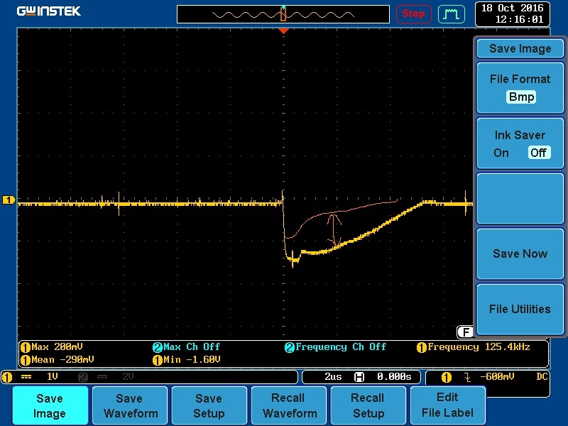
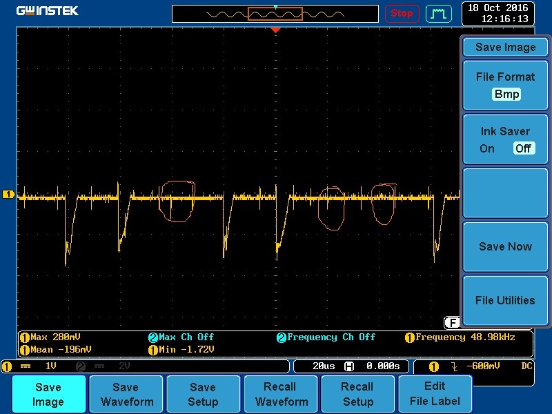
    Thanks for the reply. I am attaching two images of voltage outputs - one zoomed in and other zoomed out. DAC code sent in these cases around 0mV [i.e. I am taking an ADC output and sending to DAC via FPGA, I have seen and observed ADC output through out long on Chipscope of xilinx FPGA and have also stored on PC so ADC output is perfectly fine, no glitch there] 

    You will find negative going spike [I suspect Max carry glitch but why for so long and so high, should be within 500mV] sometimes and sometimes not. In the zoomed in pic showing only one pulse I find these spikes sometimes ending quickly within 500ns and sometimes extending. SPI Interface timing I have seen is ok.

    Again this problem is not there at all voltage levels but very selective, at some these spikes are not there, somewhere they are very tiny and voltage such as 0V 1.25V etc. they are big one.

    I am sending DAC output @ 20uS [I was sending @ 1uS but then there is lot of disturbance].

    What do you suspect. I am purposefully sending the schematic as you may get confused with lots of info in one shot. Again, if you think schema is required after all this, i will send in the next post.

    Further, I just want to know one thing as to whether Max carry glitch can be so high, can they accumulate and go even higher. Please help, client visit tomorrow.

  • Further I power up VSS [+15V, -15V] and VDD[+5V] almost together and then references, can they contribute to this, if at all?

    Regards
  • Dear Kevin,

    I think I have to give you the schematic, I have found an issue as I find similar spikes on the reference voltages as well -> TP47 and TP-48. I think I have made some mistake in connecting references of DAC and the taking DAC output as buffer. Here is the schema snapshot, please tell me. I am not using strobe terminal of AD584.

    Can I simply avoid the buffering of AD584 outputs and short them directly to VREFH-F/S together. Is buffering of references causing problem or is that way VOUT is buffered is causing problem. Please let me know. Need your help in this.

    Regards

  • Hi Kevin,

    I do not find spikes on TP45 and TP 46. Again on TP 47 and TP 48 I find spikes at some input codes and not on the others.

    A quick revert from your side will help.

    Regards
  • To clarify, what codes are you writing to the DAC when you took the oscilloscope waveforms? A quick test to eliminate any digital crosstalk from being a culprit would be configure your system to continuous write one code (ie 0x0000) and see if the glitch is visible, if it is I would suspect this is a layout or grounding problem.

    You mentioned that you are not using the strobe feature of your references, but I would verify that the -10V reference is configured properly, as the NPN's emitter should be connected to the COM pin I believe.
  • Hi,

    I have solved the problem to a certain extent by putting decaps on REF Force inputs upto 10uF. Now I do find small +/- 100mV ripples on the output and on the ref inputs but large negative spikes are a bye bye for ever.

    I think I should have added the complete provision of interfacing ref output buffered circuit to DAC as given in the datasheet but I some how got misguided by the EVM schematic and did not put additional provision of decaps between sense and force inputs and an RC decoupling network on the force inputs of the REF pins on DAC because of which I had to face a problem for at least a week but I hope I will be able to control things a lot more now.

    Regards.

  • Hi Paul,

    No writing continuous one data does not cause the glitch, it is when there is a change from 7FFF to 8000 [large spikes] or when say 80FF to 8100 [small spikes] so on and so forth. This is a clear observation after viewing things on the chip-scope.

    Again, I do not know how to strobe the negative supply reference, because I may connect the emitter output to common -10V but at the same time the logic output to base of transistor should also be connected to common but my logic output is 0 to +5V w.r.t GND so strobing is not possible according to me as I am not very good in innovating analog techniques although I understand once some one does it.

    Regards
  • I'm glad to hear that adding the capacitors to the reference pins solved the problem.  Major carry glitch of ~100mV is more inline with the datasheet curves.  Please let me know if you have any more questions.

  • Hi

    There are a few doubts that I have :-

    When I connect OP4277 outputs as per Figure 40 in datasheet:- 10uF, 1kohm, 10uF combination from Left to Right as in the figure.

    1) I get almost same performance as in datasheet where major carry glitches ranging from 100mV to 500mV and die within 100uS. How can I smooth these glitches within the scope of my schematic?

    2) I find OP4277 getting very hot specially when giving -10V output although nothing catastrophic happens - but why so hot [Am i doing something terribly wrong here in this combination]???.  IF NOT, then what can be better choice of OPAMP - Will OP4227 be better, will it not require filtering as shown in EVM [due to better drive] or whether some better OPAMP can be suggested from you?

    waiting for a revert from your side.

    Regards

  • die within 1.5uS and not 100uS - pardon typing error.

    regards
  • As far as reducing glitch is concerned, please take a look at this article which describes a few strategies. 

    DAC Essentials: Glitch-be-gone

    You could also evaluate the resistor in the feedback loop of the DAC buffer.  Consider changing the value to more closely match the DAC's output impedance.  Figure 39 in the DAC8871's datasheet shows this.

    The OPA4277 temperature is a cause for concern, ensure that there is enough headroom on the supplies as well as verify that none of the OPAMPs are operating in the rail, though I do not see anything obviously wrong in your schematic.

  • Hi ,

    Thanks for the guide. I will go through it.

    I will check the rail thing. Can you suggest me on unused opamp in the schematic - thing1 .

    Further heating has started only after adding decoupling caps on the REF inputs of DAC as I have told you- why will this be so? Any idea. If no decaps on REF inputs, there is spike but no heating. If decaps at the ref, heating but no spikes - why can this be? I hope i have cleared this.

    regards.

  • ARM arm,

    I think your reference buffers are probably oscillating, as the cap values you have on them seem very large. From left to right in figure 40, I would start with DNI, 100ohm, 1nF . Then I would check to see if the output is oscillating and what the glitch looks like. If it is oscillating, I would then populate the first capacitor with a small cap, 5-20pF. Then check the stability again.