This thread has been locked.

If you have a related question, please click the "Ask a related question" button in the top right corner. The newly created question will be automatically linked to this question.

ADS1231 noise

Other Parts Discussed in Thread: ADS1231

I'm trying to estimate the noise free resolution of the ADS1231 but can't seem to find the current noise of the PGA in the datasheet. I suppose the voltage noise is dominant for bridge circuits up to 1kOhm?

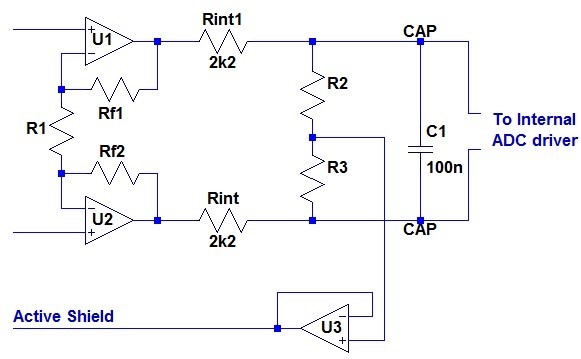
For my application a load cell with several meters cable needs to be measured with high resolution. The load cell cable runs parallel to noisy lines (pump and solenoids) therefore I plan on using on active shield. Would 2x 100k across the CAP pins followed by a low current noise/bias OPAMP as a shield driver cause any problems? The added gain error is no problem because this will be calibrated out.

Since I already plan on using x7r x2y capacitors for the input filter would it be a good idea to use them also on the CAP pins or would I be much better of using the suggested NP0 capacitor? The samples will also be filtered using software from 10sps to 1sps.

Thanks,

Koen

  • Hi Koen,

    Device characterization is done with respect to the entire ADC conversion and we do not look solely at the PGA for noise.  The analog inputs are shorted to mid-analog supply resulting in the best case scenario with respect to the noise.  This result excludes external noise effects and any reference noise with the results shown in Table 1 of the ADS1231 datasheet.

    The end result is the table values are the best possible noise performance of the ADC and excludes any additional system noise.  The external noise will be your largest contributor to the overall results due to the gaining of EMI/RFI.  I haven't heard about anyone using an active shield driver for this type of application.  The load cell output is a very small signal, and would require good stability for the active shield driver to perform adequately.  I would also be concerned about any loading effect or drift due to the cabling itself.  Also, as you've added an active component of the shield driver, that noise must also be a consideration which will be gained by the ADC.  With all these factors it would be difficult to say how well this will work, but it is an interesting idea.

    I have another thought.  What about placing the ADC at the load cell, and communicating back via a two wire interface instead of the active shield approach with the load cell cabling?

    A schematic or block diagram of what you are proposing would be helpful.  I'm not quite sure what you are referring to with respect to the CAP pins.  You cannot add any additional circuitry at this point.  This is a sensitive node and part of the filter circuit for the PGA output. We cannot easily fit a capacitor of that value on the silicon, so it is required externally.  This cap should be of high quality for lowest noise.  A film is better than ceramic, and NP0/C0G is better than X7R.

    Best regards,

    Bob B

  • Hi Bob,

    Thanks for your reply.

    The noise mentioned in the datasheet doesn't take current noise of the (P)GA since the inputs are shorted mid-supply. It would be nice to know the noise added by the load cell and external filtering due to the current noise. Since the current noise of the internal amp is unknown I can't size the input filter' series resistors optimally. Do you have a starting value?


    Below I've attached a sketch if the active shield (See Figure 13 of the datasheet). Since the differential signal is already gained up by 128 I would think these nets aren't that critical. Also in the datasheet this node is followed by a ADC driver so would have high input impedance, right? what do you think about this circuit?


    It's a good idea to place the ADC at the load cell but this would add significant cost so hopefully won't be necessary.

    Best regards,

    Koen

  • Hi Koen,

    Unfortunately we evaluate the input stage as an integrated unit to include the linear amplifier, the buffer to the modulator and the conversion noise of the ADC.  We don't split apart the individual blocks as there is no good way to quantify the individual behavior.  What you are attempting to do is outside the original design intent.  The CAP pins you are connecting in your diagram are primarily the filter of the input chopper residue.  What you may discover is increased noise pickup relative to the additional external circuitry.

    As far as using the active shield driver connections it would appear as though it should work, however I'm skeptical that you will get the performance you are hoping to get.  The first stage is a gain of 64 and the modulator buffer is a gain of 2 (total gain of 128).  As far as the input filter resistance, the largest factor to consider is input bias current due to the chopper.  I would target in the range of 1 to 5k ohms.  Generally this is not a big issue as the bridge and wiring resistance is also a part of the input filter resistance as well.

    Best regards,

    Bob B