This thread has been locked.

If you have a related question, please click the "Ask a related question" button in the top right corner. The newly created question will be automatically linked to this question.

TLV2548 SPI Timing

Other Parts Discussed in Thread: TLV2548

Hi all,

I'm having some problems with a TLV2548 not returning the correct data. To investigate this, I'm analysing the timing, especially around the SPI link in Mode 0, but struggling to understand the datasheet!

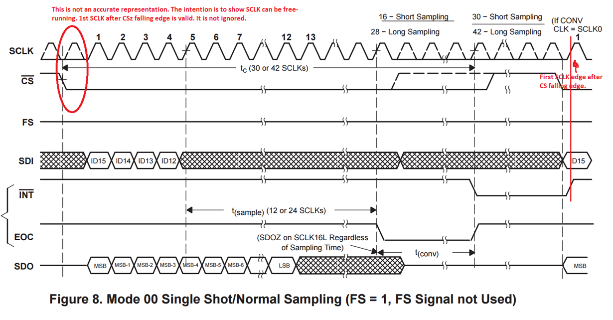
Figure 8 in the datasheet gives mode 0 operation (in my design FS and CSTART=1), but it seems to show a 1 SCLK timing delay between CS falling edge and the first SDI data being presented: is this correct, or a documentation artefact?

Also, the datasheet indicates a 42SCLK delay between readings, but again Figure 8 shows an additional delay after the 42 SCLKs before CS is raised. Does the overall SCLK timing needs to be a byte-multiplier (eg 48 SCLK)?

Any extra information on driving these chips at Mode 0 would be appreciated: I'm currently testing the chip using it's internal reference (div2), but returning millivolts range: it reeks of a 2bit-shift in the datastream somewhere!

cheers

Mat

  • Hi Mathew,

    1) 1st SCLK edge

    I have marked up the timing diagram in Figure 8 and attached below. The First SCLK edge after CS falling edge is valid and it is not ignored. You can see that in the red mark-up.

    2) Conversion frame

    a) Short sampling mode

      • First 4 SCLKs to provide channel information on SDI.
      • Sampling begins on 5th rising SCLK edge.
      • Sampling ends 12 SCLKs later i.e. on 16th SCLK and conversion begins.
      • Conversion takes 14 SCLKs i.e. till 30th SCLK counting from CS falling edge.
      • Frame ends - Total 30 SCLKs counting from CS falling edge.
      • During the first 12 clocks on the next frame you will get the conversion result.

    b) Long sampling mode

      • First 4 SCLKs to provide channel information on SDI.
      • Sampling begins on 5th rising SCLK edge.
      • Sampling ends 24 SCLKs later i.e. on 28th SCLK and conversion begins.
      • Conversion takes 14 SCLKs i.e. till 42nd SCLK counting from CS falling edge.
      • Frame ends - Total 42 SCLKs counting from CS falling edge.
      • During the first 12 clocks on the next frame you will get the conversion result.

    I hope this clarifies Mode-0 operation.

    Regards,
    Rahul

  • Dear you

    Does the SCLK is always given?Or when it is finished ,SCLK

    is setted to zero?

  • Dear you
    I wanted to know the SCLK is always given?Even finished configure?My E-mail is lanbohesky@126.com.cn
    I am a Chinese student,my English is poor,so do you understand my problems?
  • Hi,

    Thank you for your question.

    You can set SCLK to logic 0 when not reading or writing to the device.
    SCLK does not have to be active at all times.
  • Thanks very much to reply me, this picture is the timing, you just look SCLK, CS, INT, SDI, SDO,I sent it by e-mail,because I do not know how to sent picutre here
  • Hi,

    Thanks for sending the timing diagram over email. I have posted it here so that we can refer to it.

    Which mode are you operating the ADC in?
    The reason I ask this is because, when CSz = 0, there are different number of SCLKs in each frame in the image you sent.

  • Hi
    The configure order is “1010100011011011”. This means Short sampling, Conversion mode is Sweep, Sweep auto sequence is “0-2-0-2-0-2-0-2”,Pin as INT, FIFO trigger level is 1/4.Befroe configure is initializing, which I write the order is “1010000000000000”. In reading the FIFOs, I write the order “1110”,and when SCLK is falling edge, and I read 12 Bits. Like shown in the picture , the red is that the CS changes when SCLK=’0’ in the middle of it. SCLK=10M, SCLK=’0’ is 1/2 part, SCLK=’1’ is 1/2 part. And I divide it to 4 parts. Every part is 25ns, Part1 is that SCLK=’0’, Part2 is that SCLK=’0’, Part3 is that SCLK=’1’, Part4 is that SCLK=’1.The sample and conversion is after the configure, I write order”0000” and ‘’0010’’ to trigger SDI input, Sampling uses 16 SCLKs and conversion uses 30 SCLKs, when sample and conversion channel 2, I am waiting for INT=’0’ when I jump to read operations. Just as Page 17 Figure14 shown.
    The timing diagram is given by e-mial
  • Hi,

    Looking at the timing diagram which you sent over email,

    The device is operating in Sweep (10) mode with short sampling and channel 0-2 enabled. FIFO threshold is set at 1/4 i.e. 2  samples.
    As per the timing diagram, you are converting channel 0 and 2 and then INT pin goes low.

    I think the interface is working as expected.

    Could you please highlight the problem that you are facing?

    Thanks. 

  • Hi

    First think you to reply me. My problem is the data I read is not I want, I don't know why. I will send you the datas, could you help me to find the problems? Thanks very much.

  • Hi,

    Would it be possible to connect both channel 0 and 2 to a known DC voltage and then capture the data.
    I would recommend looking at the data using a logic analyzer to confirm if the output bits correspond to the digital code you are expecting.

    Once you have confirmed that the data bits on SDO are correct, we could identify the if there are any timing concerns with latching the data into the FPGA. 

    Here's what I recommend ->

    1) Connect ch0 and ch2 to VCC/2.
    2) Probe the output on SDO using logic analyzer.
    3) Confirm the data bits on SDO are as expected.
    4) Confirm the data output from the FPGA is the same as what you saw using the logic analyzer.

    I hope this helps.

    Thanks.

  • Hi
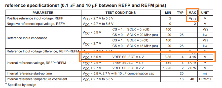
    thank you to reply me. Now I have a question: when Vcc=3.3V, can the Internal reference voltage be 4V? I give Vcc 3.3V, but I choise Internal ref 4V. I think this maybe wrong.
  • Hi,

    You will need to use VCC = 5-V for using internal reference at 4-V.
    In the datasheet, VREF = 4-V option is specified at 5.5-V supply. 

  • Hi,

    Thank you for helping me so patient. My problems has already solved. The problem is the input signal' speed shoudn't exceed the AD‘ speed. The TLV2548's speed is 80KHz in my design. So the input signal should not exceed 8KHz, or the  transition will be wrong.

    At  last, thanks Very much.