This thread has been locked.

If you have a related question, please click the "Ask a related question" button in the top right corner. The newly created question will be automatically linked to this question.

ADS1248: Calculation of resistance is about one decimal place wrong

Part Number: ADS1248
Other Parts Discussed in Thread: ADS1262, ADS124S08

Hi,

I am using ADS1248 with PT100 sensors on ports X1-X4 (3-wire RTD measurement). My communication between µC and ADS is ok, cause I read back the register values and all were ok.

I used high precision resistors on the input of the system to test the accuracy. My resistor is 164Ω ±o.1% 

I write to registers:

0x01, //Data Byte of MUX0 - burn-out current source off, selected AIN0 and AIN1
0x00, //Data Byte of VBIAS - Bias voltage is not enabled
0x20, //Data Byte of MUX1 - internal oscillator used, internal reference is always on, REF0 selected, normal operation
0x22, //Data Byte of SYS0 - gain of PGA = 4, Data Rate = 20 SPS
0x00, //Data Byte of OFC0 - write 0
0x00, //Data Byte of OFC1 - write 0
0x00, //Data Byte of OFC2 - write 0

0x06, //Data Byte of IDAC0 - DOUT/DRDY pin only used as Data Out, current source = 1000µA
0x01, //Data Byte of IDAC1 - AIN0 and AIN2 are outputs of current sources
0xff,   //Data Byte of GPIOCFG - GPIOs applied to AIN
0x00, //Data Byte of GPIOCDIR - write 0
0x00, //Data Byte of GPIODAT - write 0

My equation to calculate the resistance of RTD

R_RTD = (R_ref * final_output_code) / 2^23                    // R_ref = 820 Ohm

The problem is that I calculate a resistance of 1639.99912 Ohm . I think the resistance is shifted about one decimal place. Right value would be 163.9... Ohm.

Now my question is, is my calculation wrong or something else ?

Thanks in advance

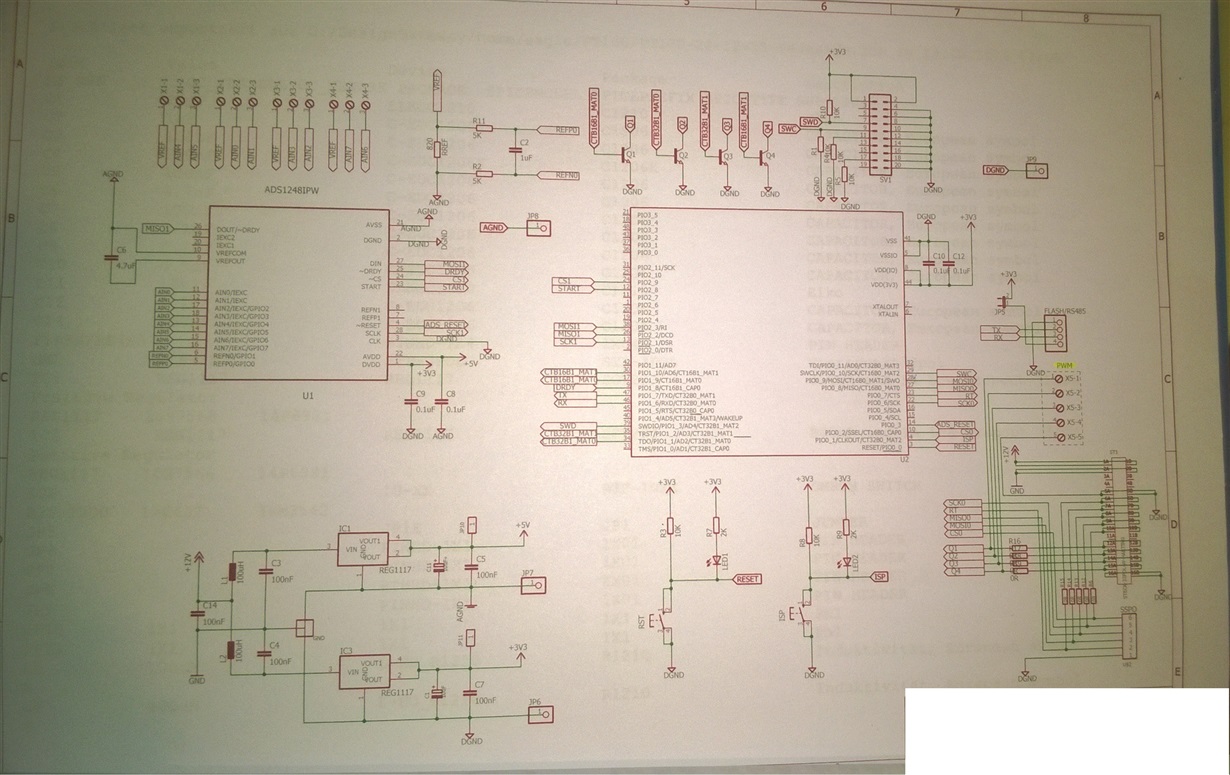
Here my layout:

  • Hi,


    It would help to have the actual data output value from the ADC to answer your question. However, I can still help guide an answer. Assuming that you have a standard 3-wire RTD configuration, where you send current to the two measurement inputs, I think result is 8x off from what you are expecting.

    Using two 1000uA IDAC currents, one IDAC current drives the RTD and one lead resistance, while the second IDAC current drives the second lead resistance. Assuming the lead resistances are equal and the currents are equal, the error from the lead resistances are cancelled.

    The IDAC currents are summed in the third lead and go to the reference resistor, so the reference voltage would be 2000uA * 820 Ohms. Additionally, you've set the PGA gain to 4, so that alters the equation as well.

    Therefore, converting the output data from the ADC to a resistance becomes:

    R_RTD = (2 * R_REF * 4 * ADC_CODE)/2^23

    This is similar to equation 25 in the ADS1248 datasheet without including the PGA gain. If you can, use a precision multimeter and directly measure the input voltage and reference voltage and see if the numbers align correctly.


    Joseph Wu
  • Thank you for your fast reply.

    the data output value from the adc is FFFFF7h.

    Tomorrow I will test out your suggestions.
  • or maybe 7FFFFFh ? at the moment I don't know which direction.
  • Hi,


    FFFFF7h is close to 0 input because the data is in two's complement notation. That value comes out to -9. Another possibility is if you've swapped the half-byte transaction reading data and reversed the nibbles, then the output would have been 7FFFFFh which means that the output is either greater than full-scale or the input measurement is open. Regardless, you may need to poke around with a multimeter to verify the voltages.

    Also, I recommend using an oscilloscope or logic analyzer to see if the digital communication is correctly reading the data.


    Joseph Wu
  • Hi,


    If you're not sure about 7FFFFFh or FFFFF7h, then I'd definitely get an oscilloscope or logic analyzer. You'll need to see DOUT and SCLK. Often, you might also want to see DIN, /CS, and /DRDY to help debug communications.


    Joseph Wu
  • Hi,

    Today I could measure the voltage of my input resistor and the reference resistor. The problem is, that there is no voltage across these resistors.

    So we can say the IDAC current sources are not active. My register values are correctly written to the ads, because I read back the values.

    My init pseudocode of my µC is:

    1. power up device

    2. wait 16ms

    3. enable the device with start  pin high

    4. set CS low

    5. wait 10ns

    6. send command (RESET)

    7. wait for 0.6ms

    8. send command (SDATAC)

    9. send initailized register values to ads

    10. set CS high

    My read function is:

    1. set CS low

    2. wait for 10ns

    3. send command (SYNC)

    4. wait for 50ms

    5. send command (RDATA)

    6. receive spi data (send 24 clocks to ads)

    7.wait for 1.8ms

    8. set CS high

    Do you have an idea what problem it could be?

  • Hi,


    First, I'd make sure that the configuration register is correctly written. It might help to read back all registers to ensure that the write has occured. Make sure the IDAC currents are turned on, and going to the correct analog input pins with the register write. The internal reference must also be turned on to enable the IDAC current sources. It's common to miss that point.

    Once you've verified the configuration register, check to see that the internal reference has indeed turned on. Use a multimeter to see that there is 2.048V from VREFCOM to VREFOUT. Then I'd check to see that IDAC current is coming out of the proper analog input pin. If it isn't, then it still might be a bad external connection of the rtd/thermistor to the reference resistor to ground (an open circuit would also show no voltage across the resistors). If you have to, take a resistor and connect it from ground to the analog pin to see if the current really is there.

    Regardless, it's still likely you have a bad setup or an incorrect circuit connection. You should be able to find it. If you can't, post back with a full schematic of your setup and the values that you are able to read back from the registers.


    Joseph Wu
  • Hi,

    I found my mistake. The GPIOCFG Register was written with 0xff, but right one is 0x00.

    Now my IDAC current sources are active.

    The IDAC current sources are set to 1000µA. R_RTD = 164 Ohm and R_ref = 820 Ohm

    As expected, my measured voltage across my RTD sensor is U_RTD = 0,164 V, and across the reference resistor  U_ref = 1,638 V.

    I read back the registers with (RREG) and got the following values:

    MUX0     0x01

    VBIAS     0x00

    MUX1      0x20

    SYS0       0x22

    OFC0      0x00

    OFC1      0x00

    OFC2      0x00

    FSC0       0x80

    FSC1       0x19

    FSC2       0x40

    IDAC0     0x96

    IDAC1    0x01

    GPIOCFG   0x00

    GPIODIR    0x00

    GPIODAT   0x00

    All values match with my written values. OK.

    My received ADC_CODE is  B32718 in hexadecimal.

    My calculation of resistance of RTD gets wrong result:

    R_RTD = 2 * R_ref * 4 * ADC_CODE / 2^23

    R_RTD = 2 * 820 * 4 * 11740952 / 2^23

    R_RTD = 9181 Ohms

    Could you find my mistake in calculation ? Is my received ADC_CODE right?

    Thanks in advance

  • Hi,


    Just to make sure you have it set up correctly, can you please send a schematic of the entire schematic? Specifically, I need to know how you have the reference resistor and the RTD resistance setup up for measurement. I'd also like to see any input filtering resistors if you have them.

    I see a couple of things wrong in your measurement and calculation.

    1. The output data is a two's complement notation. That means that the output of B32718 is a negative number and it shouldn't be. The equivalent output is -4CD8E8h or -5036264d. This isn't the correct value even if you had accidentally swapped the AIN0 and AIN1 inputs to make a negative input and the input is about 0.601 x VREF. Note that this is in a gain of 4, so it refers back to the input as 0.1501 of the reference, or about 0.246V out of 1.638V. I'll get back to this later.

    2. Starting with the voltage you measured, you have an input of 0.164V and a reference of 1.638V. If you are set up in G=4, the measurement value you should get back is:

    ADC Code = (0.164x4/1.638)x2^23 = .400 x 2*23 = 3359540d or 334334h

    3. Alternately, if you're calculating for the RTD resistance the equation should have been the input times the gain of 4, but the reference x2 because it has 2x the IDAC current. So:

    R_RTD * 4 = 2 * R_ref * ADC_CODE / 2^23

    or R_RTD * 2 = R_ref * ADC_CODE / 2^23

    However, I'm not sure why you're getting the output you get. First, find out why you are getting a negative value. Maybe you've done some conversion that accidentally gets you a negative value. Second, there might be a hook up problem. It may not be a coincidence that the negative value that you get (4CD8E8h) plus the value you are supposed to get (334331h) sum up to be close to the full scale (7FFFFFh). It's not apparent to me why that's the case right now, but it might be a setup or conversion error.


    Joseph Wu
  • Hi, thank you for your reply.

    Here is my full schematic.

  • Hi,


    Presuming that you are using the X2-1, X2-2, and X2-3 connections on your board and you have the RTD correctly connected across AIN0 and AIN1, I can't see anything that would cause your error. Have you tried replacing the RTD with just resistors to see how the values come out differently? Have you tried using any of the alternate inputs (X1, X3, or X4)? I've done a similar measurement using the 3-wire RTD example shown in the datasheet and it should be a straightforward application.

    When you take the data, are you taking a single measurement or a long series of measurements? I'd check to see if there is any change in data for a long series of measurements. There might be settling in the reference if you are switching the IDAC currents from channel to channel. Note that you have R11 and C2 which makes for a long RC time constant for settling the reference.

    There are still a few things to look at. First, make sure that your external connections are correct and that there isn't any series resistances that might cause errors in the measurement. I presume that you've done this but it's still worth going through it again.

    Can you also make sure that your AGND and DGND are the same? I'm not sure how they are connected and the AGND connection to the +5V generator is a different symbol.

    Lastly, ensure that your communications is correct. I know that you can read and write to the registers already, but it might be helpful to see the output data directly. I'd prefer a logic analyzer to read /CS, DIN, DOUT, SCLK, and DRDY but an oscilloscope might be enough.


    Joseph Wu
  • Hi,

    Now I could solve my problem. I connected my R_RTD on port X1. I needed to swop AIN5 and AIN4, so that AIN5 is the positiv input and AIN4 the negative one.

    Now I get 3339fa in hexadecimal. With your formula I get the right resistance of my RTD.

    Thank you very much for your support and effort.

    My last question is a general one. For failure cancellation I initiate self offset calibration and system gain calibration. I achieve good results with it. 

    Is there a possibility or function for noise cancellation apart from input filters?

  • Hi,


    I'm glad you were able to get your system working. I was moderately sure that the connection was wrong.

    I'm not sure I understand your question. However, I'll give an answer about your topics and hope that it covers what you're asking.

    For the calibration commands, I think it's important to run the self offset calibration, it removes some of the initial offsets that you would see in the ADC. When it comes to the gain calibration, I generally will use the default values. The default value for the gain calibration register is factory trimmed to give a low value. There may be some variation with the data rate, but in general it gives a low gain error. To run the SYSGCAL, you need to route the full scale back to the input which may not be convenient.

    If you have noise on the input, anti-aliasing filtering will certainly help. The digital filter also has the ability to remove some noise of different frequency, but you may be subject to some aliasing. If your noise comes from some sort of EMI, it also helps to have the anti aliasing so that there is some high-frequency path to ground to remove the noise. With EMI, it may also help to shield the inputs and reference to prevent EMI from coupling into your circuit.

    One last source of noise is the reference. Based on your topology, you won't have this problem. However, I've seen people use a noisy reference and the noise reflects back in the measurement. For high precision ADCs, you want to use the least noisy reference you can get for the measurement.


    Joseph Wu
  • Hi there,

    I have another question regarding the IDAC Current Sources. The datasheet says that chopping of the IDAC current sources cancels mismatches between the IDACs. How could I implement this function? Is there a standart operation of the ADS1248 or should it implemented manually as follows:

    Step 1: IDAC1 selected as output pin AIN0 and IDAC2 selected as output pin AIN1

    Step 2: measurement between AIN0 and AIN1

    Step 3: change IDAC2 to AIN0 and IDAC1 to AIN1

    Step 4: measurement between AIN0 and AIN1

    Step 5: averaging the measured values 

    Thanks in advance

    Christoph Aßfalg

  • Christoph,


    Your post describes exactly how it would be done. Mismatches between IDAC1 and IDAC2 would be averaged away with the two measurements.

    Note that you may need extra time between the measurements for setting of the IDAC driving the RTD. If there is capacitance on the inputs or the reference, you may need extra time to settle the measurement as the excitation current is swapped.


    Joseph Wu
  • Thanks Joseph,

    My other question ist about the SPI data rate between my µC and the ADS1248.

    This time I have a 2MHz transmission, before that I had 4.5 MHz. I think both worked ok. But I would like to know what you recommend?

    Could you also tell me the voltage range of the modulator (ADC) input? I need to do some calculations about it.

    Christoph Aßfalg

  • Christoph,


    In Timing Requirements table in the datasheet, the minimum SCLK period is listed as 488ns (based on a master clock frequency of 4.096MHz). That means the maximum SCLK frequency would be 2.049MHz. You shouldn't go faster than that, or there may be errors in the digital timing and communication.

    As for the voltage range of the modulator input, it should be able to take in the full input range of the ADC. However, you might be asking something different than I'm thinking. What sort of calculations do you need to do? I just need a bit more clarification on the question.


    Joseph Wu
  • Christoph,


    There was another part of the question that I think you may have removed from the post. You probably already figured this out, but swapping the IDAC current outputs and swapping the AINP and AINN measurements is not functionally the same.

    You'll want to swap the IDAC current outputs and average the results to get rid of any gain errors in the measurement caused by IDAC mismatch. If there is a mismatch in the IDAC current, then the mismatch shows up as a gain error since only one current drives the RTD, while both drive the reference resistor. By averaging both results, you remove the gain error.


    Joseph Wu
  • Thanks Joseph,

    I would like to know the value of the voltage range of ADC. My thought was that it works from 0-5V or something like that.

    Because I would like to know which voltage range is possible on my connections to PGA. Of course it depends on my gain setting of the PGA.

    In addition I want to calculate how many bits are affected of noise. Thats because I wanted to know the value of the voltage range of ADC.

    Thanks in advance

    Christoph Aßfalg

  • Christoph,

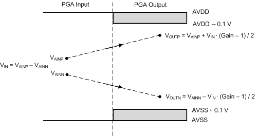
    The voltage range for the ADC is listed as equation 3 on page 26 of the datasheet. As you mentioned, it does vary with the gain of the ADC.

    When the gain is 1, the input range is AVSS+0.1V to AVDD-0.1V. However, when the PGA is in gain, then you must also account for the output range of the PGA. If you look at the diagram below, it helps illustrate that the PGA output range must be considered as well.


    I'm not sure I understand your last comment about how many bits are affected of noise and the PGA input range. If you clarify the comment, I may be able to address it.

    Joseph Wu

  • I got it. Thank you very much.

    I also have questions about the system offset calibration and system gain calibration. 

    Currently I am perform Self Offset Calibration and System Gain Calibration.

    Before sending SYSGCAL command I change the last 3 bits of MUX1 register to Gain calibration.

    After SYSGCAL command I change MUX1 again to normal operation.

    1. Is there a difference between Self offset calibration and System offset calibration?

    2. is it plausibel that all three OFC registers are all filled with 0x00 after Self Offset calibration?

    Thanks Christoph Aßfalg

  • Christoph,


    There is a difference between self offset calibration and system offset calibration. In self-offset calibration, the ADC inputs are shorted in the multiplexer and the ADC is run to find what the output value is. The output of the digital filter is averaged and stored. This result is then subtracted from future results to act as an offset calibration.

    The system offset calibration is a bit different. The user takes the system input and zeroes the input. Imagine if you have an amplifier on the front end with an inherent offset. You would zero the inputs at the amplifier and this amplifier offset is seen at the ADC input. However, this would be your system offset that you would calibrate out.

    As for the second question, it is unlikely that all three offset calibration registers read 00h. However, this may depend on the PGA gain and data rate. At higher data rates, you would see more noise. Even when the inputs are averaged, you'd generally see enough noise to show at least some change in the offset calibration register (at least the LSB). There is also some change in the noise for different PGA settings, but I still find it unlikely that anything will get you a 000000h offset reading.

    I do have one other note on your calibration. In general, the system gain calibration isn't necessary. The gain error is trimmed at the factory for the different PGA gains. The gain error is typically 0.005% (max of 0.02%). It's true that you may be able to do better with a system gain calibration, but I'd measure the resulting gain error with corroborating measurements with a precision multimeter.


    Joseph Wu
  • Hi Joseph, 

    Thank you a lot.

    Now I could handle my problem with my OFC registers. The wrong calibration time was used.

    Another thought of my is:

    - I use all 4 differential Inputs on the ADS1248

    - On page 73 in datasheet ADS1248 it says that unused analog inputs should be connected to mid-supply or AVDD to minimize leakage current. 

    -  is it helpful while measuring takes place of one RTD sensor, that the other RTD sensors in this time are connected to mid supply (write to vbias register)? (to minimize leakage currents)

    Thanks 

    Christoph Aßfalg

  • Christoph,


    You could put the unused analog inputs at mid-supply to reduce leakage currents. With this mux there might be a change of a few nA seen at the analog inputs being used. However, this might not be necessary for you. The leakage current is more of a problem when there are large resistors at the input (like resistors used for input filtering.


    Joseph Wu
  • Thanks Joseph,

    Now I am thinking to improve my schematik of ADS1248 because I don't need to measure the range of -200°C to 850°C. The temperature range of -50°C to 250°C would be enough. Precise measurements schould be done in the range of 90°C to 250°C. My goal is a minimum resolution of 0.01 °C.

    Currently my DVDD is 3.3V and AVDD is 5V.

     - what is the difference of taking AVDD to 3.3V or 5V? (only PGA input range is bigger?)

               - what are the advantages or disadvantages of taking 3.3V or 5V?

    I also read that the reference voltage is best taken at mid-supply. I think that AVDD is meant at mid-supply for best performance?

    Christoph Aßfalg

  • Christoph,


    Sorry, I was out of the office for the last half of last week.

    First, if you want an accuracy of 0.01°C, then make sure you do some sort of error analysis about what kind of resistive error that you might see, and how that translates that to resistive errors.

    As for the other questions, I don't think there's much difference between 3.3V and 5V. However, if you have a choice, go with the 5V supply. I think the noise performance is slightly better (comparing Table 3 and Table 5 in the datasheet). Also, having a 5V supply maximizes the reference and input range of the ADC. This will maximize the signal compared to the noise of the device.

    For your last comment, you mention that you read that the reference voltage is taken best at mid-supply. Assuming that you are describing the application example, this is just so that the RTD measurement is set near mid-supply since the reference acts as a level shift to raise the input voltage near the middle of the input range, allowing for the PGA to maximize the gain, without clipping the PGA's output range. Since the PGA supply comes from AVDD, the PGA input range is specified as a function of AVDD.


    Joseph Wu
  • Thanks Joseph,

    in datasheet page 86 of ads1248 it says on 10.3 "Do's and Don'ts" that you should use a single ground plane for analog and digital grounds.

    What's the reason for that? the advantage?

    In my current board I have separat ground planes for analog and digital ground because of separating noise.

    AVDD = 5V and DVDD = 3.3V

    Best regards Christoph Aßfalg

  • Christoph,


    I'm going to refer you to this page that covers grounding:


    I'm sure that if you separated the ground planes and connected them back at the ground coming into the board, it would be fine. It's just our recommendation. By using a single ground plane, you eliminate possible ground loops and you give the lowest impedance path for the ground return.

    However, you're right in that you might create noise problems from the analog and digital ground planes combined. To counter that, you'll still need to carefully consider how you lay out your board. Analog and digital portions should be separated and not cross over each other's sections of the board. Route your lines carefully and check over your completed routing for signal integrity.


    Joseph Wu

  • Thanks Joseph,

    This time I am doing some calculations about my new design to reach the 0.01°C accuracy. 

    I want to take a resistor on AINN (TI call it Rzero) to shift the minimum measurement value. 

    My goal was to measure from -50°C to 250°C.

    In my current design I took: Rref = 2.5kOhms (Tol. 0.01% and 0,2ppm/°C), Rzero = 150 Ohms(Tol. 0.01% and 2ppm/°C), I(IDAC) = 1000µA, PGA Gain= 32 V/V

    So I actually get a measurement range of -70°C to 340°C -> okay

    So far so good, but when I am doing Error calculations it is hard to reach my aim of 0.01°C accuracy.

    I am performing error calculation including Temperature Drift. 

    In the TI Design sheet "3-Wire RTD Measurement System Reference Design,
    -200°C to 850°C" it says on page 18: "After removing the IDAC mismatch errors with chopping, a two-point gain and offset calibration can
    remove the errors from the RREF tolerance, offset voltage, and gain error, leaving only the error from INL."

    -But in the datasheet it says the offset voltage is minimum -15µV and maximum 15µV after calibration. So I think this could not be cancelled from the error calculation?

    VIO Offset voltage (input referred) After calibration(1) –15                                                    15 μV

    - My other question is how R(zero) can be handled due to the error calculation? Is the Gain error cancelled after calibration, too? and is Gain Error calculation caused due to R(zero) Temperatur Drift the same calculation as  Gain error Temp. drift due to Rref?


    - How can I calculate the self heating Error from R(RTD) ?


    - is it plausible to sum the error calculations with the noise error?


    So much questions, I hope you can help me


    thank you 


    Christoph Aßfalg


  • Christoph,


    I'll try to address your questions as they come up in your text.

    I think is some of our older literature, we've used these Rzero to shift the measurement so that it centers around a zero voltage. This would make the measurement bipolar so that a larger PGA gain could be used and the resolution could be increased. However in practice, I think this would be very difficult. Rzero would have it's own resistive error and drift, adding more error to a system that requires a lot of calibration. There might also be parasitic resistances associated with soldering down an extra resistor and the additional trace resistance. Generally, I would avoid it.

    Again, I'd say that 0.01°C accuracy requires a lot of calibration. When I say calibration, I don't necessarily mean using the SELFOCAL and SELFGCAL commands. I mean that you need to use precision resistors to make measurements to find the exact offset and gain errors in the measurement. In the TI design, we use precision resistors to simulate different RTD resistance values over temperature. I think it would require a similar method to determine the gain error and offset. Using this you could calculate values for the OCR and FSR. While a SELFOCAL might get you to 15 uV in offset, you would likely need to determine a more exact offset value with measurement.

    Again, I'd advise not using Rzero as part of the measurement. As I mentioned earlier, additional parasitic resistances may be a factor, and an extra 100mΩ would be a huge error.

    For self-heating error for the RTD, I think you'll need to look that up from the RTD manufacturer. The amount of self heating depends on the power dissipation in the RTD and dissipation constant to the ambient temperature.

    I think it is possible to resolve the noise error and the error in measurement. When making a measurement with the ADC, there may be an error associated with the noise. However, often the noise is still something that can be averaged. By taking n averages of the measurement, the noise standard deviation should reduce by a factor of √n.

    I would point out that the TI design was shown mostly using calculations to Ohms, showing how much the ADC might be in error. However, it doesn't really consider the error from the ADC itself. The TI design in slau520 is really designed for a ±0.05°C level.


    Joseph Wu

  • okay I understand.

    Last days I was doing error calculations of various concepts.

    I attached the best one to this writing.

    Could you please check if it is correct and possible to realize? Sometimes it is German but in most cases it is in English and the calculations too.

    With calibration I would reach a 0.047°C accuracy including temperature drift. This is better than the old design.

    Thank you in advance.

    Christoph Aßfalg

    Konzept 1.pdf

  • I have another question regarding your other ADS products.
    Is there a better IC maybe for lower noise performance, Offset Error of ADC drift, Gain Error of ADC drift and INL Error of ADC?
    To get better accuracy than the ADS1248. I am thinking of ADS124S08 or ADS1262.

    Thanks Christoph Aßfalg
  • Christoph,


    The ADS124S08 is considered the next generation of the ADS1248 and it does have some improved specifications. The ADS1262 is also a fine part, with a good noise performance. If you look in both datasheets, they have sections with example designs showing the performance of the device when measuring RTDs.

    If you read through the example designs, I think they both may have similar performance to the ADS1248, although I think the ADS124S08 and ADS1262 might be a bit better to achieve the specifications. The noise performance and integral non-linearity in measurement are better in both devices.

    However, I'm still concerned about your desired accuracy. From your last post, and accuracy of 0.047°C is difficult to achieve. Have you considered the error of the RTD itself? A DIN Class A RTD has a listed error of ±(0.15 + 0.002*|T|)°C. There are RTDs with much higher accuracy and performance, but even with a 0.01% DIN RTD, the error starts at 0.01Ω and increases from there. The datasheet example designs use 0.01% and 0.005% precision resistors to make measurements to verify the designs (and the resistance values are still measured back to verify the value). Even with the highest accuracy RTDs, you'll be at this level.

    I'll read through your error analysis. At first glance it seems similar to the analysis from the TI example design shown in slau520.


    Joseph Wu
  • Hi Joseph,

    What does noise performance in the datasheet of ADS1248 mean? Is this only the noise of ADS1248? 

    Are this noise values the best ones you can achieve on this ADS1248?

    Thanks Christoph Aßfalg

  • Christoph,


    This noise would be measurement from just the ADS1248. I would say that this is close to the best case noise, certainly without any contribution of noise from the reference in the measurement.


    Joseph Wu