This thread has been locked.

If you have a related question, please click the "Ask a related question" button in the top right corner. The newly created question will be automatically linked to this question.

ADS1281: Discrepancy between test signals and converted data

Part Number: ADS1281
Other Parts Discussed in Thread: OPA1632

Hi,

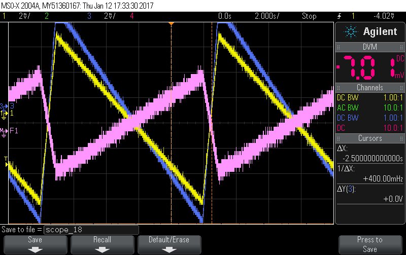
I am testing an ADS1281 with a triangular wave signal. My problem is that converted data show a strange type of distortion near zero. I connected oscilloscope probes to both inputs of the ADC and I saw regular triangular waves, without distortion. The sampling process lasts less than 1us, so I know that what I see on the oscilloscope is not what the ADC is measuring in reality. My guess is that the antialiasing filter causes this problem because of its high common mode impedance, but I do not know how.

Below you can find:

1. a screenshot of the oscilloscope (yellow = negative ADC input 2mV/div; blue = positive ADC input 2mV/div; pink = difference between positive and negative 1mV/div);

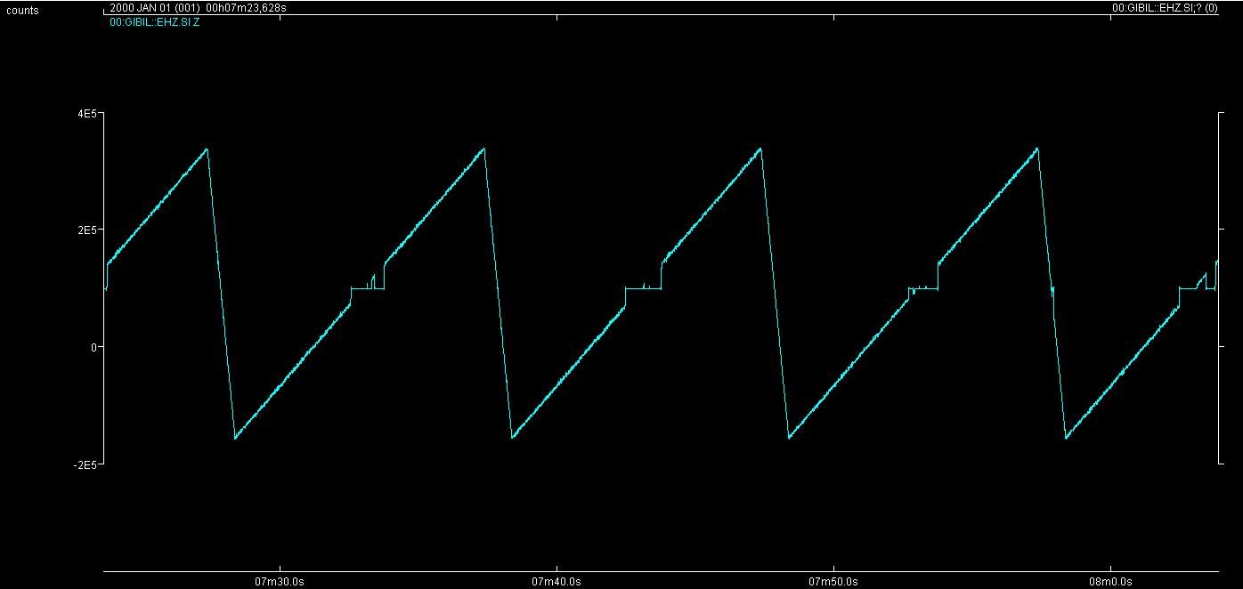
2. A picture showing converted data

3. A schematic view of antialiasing filter that shows a some details of the test setup.

My next step will be repeating the same test with another board that has an active anti-alising filter instead. If anyone can help with the passive filter case depicted above I would really appreciate it.

Regards, Gioacchino

  • Gioacchino,


    I don't normally cover this device, but I suspect that you are correct that this problem is caused by the anti-aliasing filter. As a test, I would replace the 10kΩ resistors used for R1 and R2 with shorts or something near 100Ω.

    For this device the input impedance is rather low (55kΩ). In reality, this is not a constant input impedance, but rather an equivalent impedance created as the input is capacitively sampled and charge is periodically carried away. If there is large series resistance as you have in the anti-aliasing filter, the capacitors sampling the input may not settle correctly and it may appear as a large non-linearity error near 0 input.

    I would note that with such large filter resistances, and an ADC low input impedance, you'll already have a very large gain error.

    If you're interested, look at the ADS1281 evaluation module users guide and find the schematic. I believe that it uses an OPA1632 as part of the input filtering.


    Joseph Wu
  • Gioacchino,


    Also, remove R5 as part of the test. It is also taking charge away from the input sampling. If this lowering R1 and R2 help improve the problem, then you might try adding R5 back in (I missed R5 in the previous look of your schematic).


    Joseph Wu

  • Dear Joseph,
    you wrote:"If there is large series resistance as you have in the anti-aliasing filter, the capacitors sampling the input may not settle correctly and it may appear as a large non-linearity error near 0 input". I would really like to understand more about that. Is there any reference about this topic that I could read?

    Concerning the effect of the antialiasing filter on settling time, why do you focus only on filter resistors neglecting capacitors? In my opinion, during the sampling phase, this capacitors can be seen as constant voltage sources and the settling time should be determined by R3, R4 and the ESR of C3.

    If the distorsion were caused by ADC input equivalent impedance, becoming too low near zero, I would expect to see a similar effect with the oscilloscope, because the equivalent impedance is derived from a time averaged model of a switching capacitor circuit. For example, the effect of the equivalent impedance of a charge pump can be measured even with a multimeter, that is a device with a definitely low measurement rate...

    Please let me know what do you think about...

    Best regards, Gioacchino
  • Hi,
    the board with amplifiers does not show any sort of distortion near zero. However I am still interested in finding out what goes wrong with the passive filter case, so if anyone can help I would realy appreciate that...
    Regards, Gioacchino
  • Giacchino,


    This effect is similar to a "dead zone" behavior which can happen if the op-amp gain in the modulator is low, or if there is leakage in the sampling. In the case of a high series resistance, the charge transfer from input sampling is similar to a leakage.

    I focus on the filter resistors because the effect isn't just a simple RC case. The input sampling switches in the sampling capacitor from the ADC in parallel with the filter capacitor.

    As an example, you have 100nF on your inputs, when you have a 16pF capacitor (I'm simplifying figure 36 in the ADS1281 datasheet) the voltage seen at the input will momentarily drop as the charge in the 100nF capacitor drops to fill the 16pF capacitor. It should immediately drop 0.016% from the initial value as the charge is redistributed from the full 100nF capacitor to the empty 16pF capacitor. After the input sampling capacitor is switched in, you have one modulator period (1us) to settle the circuit from the input before the filter to make up that small difference. This occurs each modulator period at a 1.048MHz rate.

    If you were to reduce the input series resistance and increase the capacitance, then you have a larger input capacitance from which to draw charge. If the input capacitor is 1uF, then the voltage across the sampling capacitor drops 0.0016%, leading to a smaller sampling error. You'll still have the same overall RC time constant, but you'll have less error in the sampling.

    Of course this is a simple explanation, and sampling into the modulator is a bit more complicated. The point is that using a larger capacitor will supply more charge into the sampling capacitor so the error will be smaller.

    This "dead zone" isn't going to be seen with the oscilloscope. This problem comes from an error sampling the input into the modulator, and is not an external effect.

    Out of curiosity, approximately how many codes is your dead zone error, is seems like it might be about 100 codes. Is that correct? How much is that in voltage. I wasn't sure if your y-axis deviation was correct.


    Joseph Wu
  • Gioacchino,


    I would look up dead zone with Delta Sigma modulators. There is some reference to this in "Understanding Delta-Sigma Data Converters" by Richard Schreier and Gabor Temes but I'm sure you can find more information on it.

    Again, I think the large series input resistance in the filtering causes a similar effect to this, and it should go away with a lower series input impedance.


    Joseph Wu
  • Dear Joseph,
    starting from your hints, I am going to do a research on the topic of dead zones in Delta Sigma modulators. I agree with you on the cause of the problem, that is too high filter impedance, but I would like to understand more...

    To answer your question, in the portions of data affected by distortion, the noise power is extremely low, well below the value desumible from the datasheet, in fact only 6 of 32 bit are variable in those areas.

    Regards
    Gioacchino Fertitta
  • Dear Joseph,
    after reading something on this topic, maybe I am starting to picture what happens inside the modulator.

    When a very small voltage source is applied to ADC inputs, the modulator starts producing a tone whose period is 2 times the sampling period, something like "01010101...". The tone is unaffected by input level, as long as input value stays within a small interval called dead zone. In normal conditions the dead zone width is so small that even device noise can take the modulator out of it.

    When the filter resistance increases however, the open loop gain of the modulator decreases, leading to an increase in dead zone width.

    In my case: the tone would explain why so little noise power is left in the signal band (only 6 of 32 bit flickering); the relation between open loop gain and dead zone width would explain why filter capacitors, as big as they are, are of no help. In fact only the low frequency portion of transfer function would matter.

    What do you think about?

    Regards, Gioacchino
  • Giacchino,


    With large series resistances, I think of it as the input charge never reaching the integrator similar to a case if there is a leakage before the integrator. This will have the effect of seeing 0V for input with any small amount of signal draining away from the integrator during each sample. The modulator would alternately feed back the reference and the negative reference, giving the alternating 101010....

    Operationally, the important part is how much error is there after the modulator sampling and does the input sampling settle in a single modulator period.


    Joseph Wu
  • Dear Joseph,
    I would like to thank you for your support and patience.

    I made some other tests, the ADC stays in the dead zone even when ADC inputs are connected directly to ground. It can be seen by looking at noise power that is too low. I think that this behaviour is in accordance with your explanation, but shorted input noise measurements are reported in the datasheet so it should be possible to do these measures...

    Do you think I can have some board layout problem?

    Regards, Gioacchino

  • Giacchino,


    Just to be clear, you have removed the series resistances, shorted the inputs together, and then tied the inputs to ground? If this is the case, then I'm not sure what is wrong. I would have expected the input noise to read similar to that listed in the datasheet.

    I did talk to one of the engineers that has worked with this device. He did say that generally, an input buffer is recommended. If you look at the ADS1281EVM, the OPA1632 is used for filtering/buffering. However, regarding the noise from the datasheet with inputs shorted, those results are with the buffer bypassed, and inputs are shorted to ground similar to the method you describe.

    I'm not sure what would be different between your setup and what we've used. However, the setup used in the EVM is a good place to start. In general, the EVM user guides have good information about the setup, schematic, and layout for the device.


    Joseph Wu
  • Dear Joseph,
    you understood well what kind of setup I used.

    I know the evaluation board even though I have not replicated the circuit. I verified power supply (+2.5V and -2.5V analog; +3.3V digital), voltage reference (4.096V between VREFP and VREFN, VREFN to AVSS), master clock (3.3V, 4.096MHz) and everything looks fine...

    In my application, the power consumption matters a lot. Togheter with SNR it is the first figure that each user will look at. This is the reason why I am so interested to a passive filter. I know that there are plenty of micro power amplifiers but if you consider the noise performances and the flicker noise level of each, the number of suitable devices is not that high.

    The key point is that: if data are not ok then something is surely wrong with the board, I just have not found it yet... I will make more tests and if I have other questions I will ask you again.

    Thank you for your support.

    Best regards, Gioacchino

    Regards, Gioacchino
  • Dear Joseph,
    I got It, it was the voltage reference circuit. I implemented an active filter in order to reduce reference noise.

    The assembly of this circuit did not follow the design and, as a result, the output impedance were high above 100kHz...

    The dead zone disappeared after that the assembly error had been corrected.

    Regards, Gioacchino