This thread has been locked.

If you have a related question, please click the "Ask a related question" button in the top right corner. The newly created question will be automatically linked to this question.

PGA411-Q1: issues with PGA411

Part Number: PGA411-Q1

Dears,

I occur some issue with PGA411, please help to give some advise.

Issue 1: the ripple of the BOOST is too big.

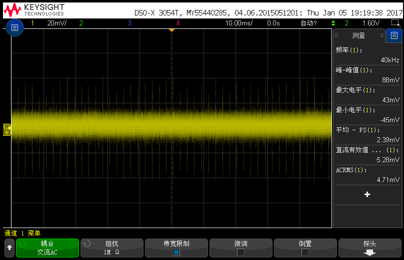
We boost 6.5V to 12V to supply power to the VEXT. The ripple of input 6.5V is less than 100mV, while the output ripple is about 650mV .

Input ripple:

output ripple:

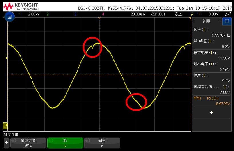
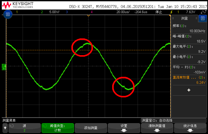
Issue 2: the output of the exciter-amplifier distorts.

As the graph below shows, there are two peaks in the red circle every cycle. And the sine degree of the wave is not good.

Wave of OE1:

Wave of OE(differential wave)

Issue 3: The FAULT pin will turn high without the resolver. the SFAULT of  DEV_STAT4 is 1, while the other bit are all 0. So I can't get the Fault type.

  • The appropriate Applications Engineer has been assigned to respond accordingly. Thank you for your patience.
  • Luffy,

    I have a couple of questions about your test set-up:

    1. Are you using the unmodified EVM for these tests? If not, what does your boost circuit look like (inductor and capacitor values)
    2. What load are you using for the resolver? How much output current are you driving?

    Issue 1: I'll address this once I hear more details about the set-up.

    Issue 2: It looks like you don't have enough room between the power supply rail and the positive peak of the OE signal. Try increasing the boost voltage and some of the distortion should clear up. The distortion will also be worse for higher loads, so I am curious what load you are using. Also, I can see the ripple from the boost in your OE waveforms, so once we reduce the ripple, the waveform should look cleaner.

    Issue 3: Are you saying that the FAULT pin will go high when you disconnect the resolver? That is expected behavior, but you should be able to see the fault status bit set. Please note that the fault status bits are clear on read, so if you read them more than once, you will see the behavior you are experiencing (where only the SFAULT bit is set).

    Thanks,

    -Clancy
  • Hi Clancy,
    I am the colleague of Luffy.
    About the questions,
    1.We are using our own demo board for the tests, we design the board according to the TIDA-00796 reference design.
    The boost circuit has an inductor of 47uH/2.5A and two 4.7uF/25V/X7R ceramic capacitors and one 0.1uF/50V/X7R ceramic capacitor.
    2.The parameter of the resolver we are using are like this:
    exciter voltage: 7Vrms(but we are using in 4Vrms mode in order to reduce the current and temperature rise)
    exciter frequency:10KHz
    input impedance: 64±10 ohm(this is given by the manufacturer, the actual current is less than 140mA, because we set the EXTILIMTH_L1_2 and EXTILIMTH_H1_2 of the DEV_OVUV1 register to 140mA and 150mA, no fault occurs)

    Thanks
    -Howard
  • Howard,

    - Is the distortion on the OEx signals still happening when you change to 4VRMS mode? In 7VRMS mode, the 12V boosted voltage may be too low, which would cause some distortion.
    - Like the TI Design, do you have the footprint for the diode between GND and the VSW pin? Adding this diode sometimes helps with this type of issue, so please try to add it if possible.

    Thanks,

    -Clancy