This thread has been locked.

If you have a related question, please click the "Ask a related question" button in the top right corner. The newly created question will be automatically linked to this question.

DAC7811: 0 to 5V Output Schematic

Expert 1961 points
Part Number: DAC7811
Other Parts Discussed in Thread: LM7705, REF5050, OPA376, OPA727, DAC8811, THS4011, LM4050-N-Q1

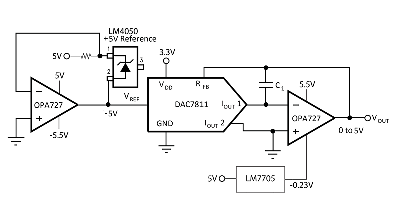
I need a 0 to 5V output from the DAC7811.  I figured out a solution that I think will work, but I would appreciate it if someone would please review my schematic.  I based it off of Figure 29 in the data sheet.  I used an LM4050 5V reference since I am already using it in an existing product.  If it isn't ideal I could use something else.  The reason I included the LM7705 for the negative supply of the output op-amp is only because it made me feel better that the output would never go very far negative if the circuit failed.  Maybe I'd be better off using the -5.5V supply and putting a Schottky diode clamp to ground on the output to prevent it from going too far negative.  VDD of the DAC7811 is 3.3V because that is the interface voltage to the FPGA.

Here is the schematic:

Any advice would be greatly appreciated.

Greg

  • Howdy Greg,

    Thanks for posting to e2e.  I don't see any issues with the circuit presented, I've notice that you used the shunt to regulate a negative reference supply.  One thing to note is that the LM4050 device has a maximum operating current of 15mA. Therefore 5V/R, should be less than this value.  I understand your concern about the output saturating to the negative rail, but I've only seen this when one of the op amp inputs is disconnected or is left floating.  If the connections are robust, I don't see any reason for not sourcing a negative rail (if one is available) to the operational amplifier.  Additionally, if the op amp is true rail-to-rail you can simply connect the negative rail to GND, it should have no problem producing a unipolar output.

    Hope this information helps.

    Best Regards,

    Matt

  • Hi Matt,

    Thank you very much for looking it over. I'm glad you didn't find any issues. Multiplying DACs were confusing at first, but I think I understand them pretty well now and they are pretty cool. Definitely more work than a DAC with a buffered voltage output. I am on a tight schedule and don't have time to breadboard it, so I couldn't afford to make a major error in the design. Thanks again for looking it over. I can handle some cuts and jumpers, but not a complete redesign. My forum posting would have been avoided if the data sheet explained the limitations when producing larger output swings directly using that method. It was explained that an inverting amplifier is not used on the output because of resistor tolerances, which makes sense. The circuit for 0 to 2.5V was presented without any explanation of limitations, so I was just being careful, just in case there were some subtle limitations I wasn't considering. Thanks for pointing out the current limitation of the LM4050, and also for boosting my confidence about circuit failures causing the output to swing to the negative rail. Since I have a negative supply in the system already, I think that is the best solution.

    Best regards,

    Greg
  • Hi Matt,

    I was looking at this again and wondering whether the op-amp driving the VRef of the DAC7811 needs to be used when using a shunt reference like the LM4050? The minimum input impedance of the DAC7811 is 8k, which means the load current would only be -5/8000 = -0.625 mA worst case. That is well within the maximum 15 mA spec of the LM4050. I had followed the suggested circuit in the DAC7811's data sheet, which is why I drew the schematic like I did. But now I am wondering if the author of the data sheet used the op-amp because a shunt reference is inferior? Or perhaps they didn't think of using a shunt reference which can produce a negative output from a negative supply. I think it simplifies and reduces the cost of the circuit to use a shunt reference.

    Thank you and best regards,

    Greg
  • Let me ask the question in a different way. In the data sheet for the DAC7811, there is an example circuit for creating a 0 to 2.5V output using a single +5.5V supply. The reference is a REF5050, which is buffered by an OP376 op-amp. Since the REF5050 is capable of outputting +/- 10 mA, and the load is under 1 mA, why is it necessary to buffer the reference? Is it because of the glitch energy? If so, why wouldn't bypass capacitance be able to supply the glitch current? Is the issue that the REF5050 needs a capacitance with a 1.5 Ohm ESR, which is quite high? I looked at the noise specs for the LM4050 and REF5050 and one is specified from 0.1 Hz to 10 Hz, and the other is specified from 10 Hz to 10 kHz. I'm not sure how to compare the two. Is the LM4050 noisier than the REF5050? The LM4050 can be heavily bypassed, which means the output should do OK when the DAC glitches. Wouldn't a bypass capacitor be able to supply charge more quickly than an op-amp?
  • Hi Greg,

    Sorry for replying late. The buffer is used at the output of the reference source for load regulation, not for noise or glitch. As the DAC7811 doesn't have a buffer at the reference input, it will draw a code-dependent current from the reference source. If we don't have the buffer, the actual reference voltage will change based on the output current, which is specified in the datasheets of the reference source, either as a graph or a ratio. This is true for both LM4050 and REF5050, though the values are going to be different. With the buffer, the reference always sees a high-impedance load all the time and will therefore have least drift because of code change.

    Hope that answers your question.

    Regards,
    Uttam
    Applications Engineer, Precision DACs
  • Hi Uttam,

    The DAC7811 is a multiplying DAC with an R-2R ladder. Doesn't that architecture present a constant impedance of R Ohms? In that case the current required from VRef is code-independent.

    Regards,
    Greg
  • Hi Greg,

    You are right. It was a mistake from my side in my last post. You see a constant impedance looking from the reference. So, the buffer is not used for code-dependent current. Considering the static scenario, there can be voltage drop on the trace between the reference and the DAC due to the current drawn from the reference source. One way is to put the reference very close to the DAC and the other way is to use a buffer with the feedback loop in Kelvin connection so that the error due to this drop is eliminated. There can still be errors due to transient conditions due to switching. The buffer takes care of that as well. However, as you rightly pointed out, this can be taken care by putting a capacitor very close to the reference pin.

    So, ideally, you can manage without the reference buffer. But, if you need better performance, you should use it. On one hand, the buffer isolates the DAC load from the reference. On the other hand, it also introduces its own drift and noise. Hence, you need to make a trade-off.

    Regards,
    Uttam
  • Thanks Uttam. Let's assume that a shunt reference is placed very close to the VRef pin of the DAC. That eliminates a voltage drop as a source of error. Why does the buffer offer better performance? I looked at the glitch noise in Figure 10 of the data sheet, and I estimate the frequency to be in the range of 3 to 10 MHz or so. The impedance of a bypass capacitor is very low at that frequency. Can a buffer keep up with a bypass capacitor at delivering charge at that rate? I estimate the slew rate to be about 3 to 4 V/us. The OPA376's slew rate for G = 1 is 2 V/us, so it can't keep up with the glitch. But maybe that is actually a good thing in this case because it would filter it out a little bit.

    In Figure 10 of the DAC7811 data sheet, would you please explain where the output voltage is measured? Is that at the output of a high-performance op-amp? Or at the inverting input of the op-amp?

    Thanks and regards,

    Greg
  • I found a paper from Texas Instruments named "Sample & Hold Glitch Reduction for Precision Outputs Reference Design" (www.ti.com/.../tidu022.pdf). On page 35 and 36 it describes the reason for the glitching in R-2R DACs. It says "the main parasitic capacitors affecting output performance are the gate-to-drain capacitances, Cgdn and Cgdp". How important are the internal "A" and "/A" signals compared to VRef at charging and discharging those parasitic capacitances?

    Thanks and regards,

    Greg

  • Hi Greg,

    Sorry to introduce a third TI "face" in this thread, but I thought I might offer some quick insight on this...

    I wrote a couple of reference designs with, at the time interns, using multiplying DACs. In some of those designs we experimented with more or less exactly this by adding optional reference buffers to see what kind of effects inclusion of the buffer might have on the transient, or dynamic, performance of the DAC - things like glitch, settling time, etc.

    The short of it is that we weren't able to observe any appreciable benefit of the buffer versus simple "charge-well" / decoupling capacitor approach when a low-bandwidth precision amplifier was at the output of the DAC, basically something similar to the OPA727 in your proposal. If you look in the DAC8811 datasheet for example most of the AC characteristics are measured with a THS4011 - a high-speed amplifier with GBW 290MHz. In this case, the buffer is somewhat helpful in measuring these dynamic specifications.

    In the typical case of using the DAC for DC or precision applications, the buffer amplifier is not necessary. Local decoupling is sufficient.
  • Hi Kevin,

    Thanks for joining the discussion and offering your experience.  I'm sorry it has taken so long to reply.  The past few days have been really busy for me and I haven't had the time to give this the careful thought it requires.  I'll start by stating the conclusion I came to after writing this reply.  Then I'll follow it with things I thought about before I came to this conclusion.

    Unless I'm mistaken, you were not comparing shunt references to 3-terminal references.  You were probably comparing a circuit that used something like a REF5050, with and without a buffer op-amp.  I am thinking that the answer to my question is that a LM4050-N-Q1 will work fine without a buffer if the performance of that reference is adequate.  Since the REF5050 is a 3-terminal device, a buffer would be needed in order to turn it into a negative reference by creating a virtual ground.  But in the case of the reference design of Figure 33, the buffer could be optional since the REF5050 is used as a positive voltage.

    I've been thinking about the things you said, and one realization that I came to is that I think about things digitally, since that is mostly everything I've worked on in my career.  In digital electronics, a clock event happens and the bypass capacitors do their thing and then they charge up in time for the next clock event.  But in electronic circuits that convert digital signals to analog, there is life between clock events.  If the DAC requires charge on the VRef input due to the rollover glitch event, charge will come from the bypass capacitor (assuming the glitch involves VRef), but then the reference needs to resupply the capacitor with charge.  In the meantime, VRef has drooped and the analog output from the DAC will have changed.  More capacitance will make the droop less pronounced.  In a digital system it doesn't matter what happens to the supply as long as all of the digital signals retain their proper state.

    I looked at the transient performance of the REF5050, and the graphs in the data sheet show a relatively small spike in the output for a step change in current.  Interestingly, the output voltage spike is lower for a larger spike in current demand, suggesting that a short-lived (but high amperage) glitch event in the DAC would be handled fairly well by a REF5050 with generous capacitance on its output.  But the time scale in those graphs is 20 us per division, so perhaps the voltage spike is larger than the graph shows.  In one graph the spike is off the chart.  The DAC7811 glitch event is on the order of 100 ns long, which is quite a bit shorter than what can be seen in the chart.

    I'm still unsure about what drives the glitch event most.  Is it an internal issue with driving the parasitic gate-to-drain capacitances?  Or is it because of limitations of VRef?  If it is internal, then there isn't much that can be done about it, short of choosing a different DAC or employing a sample and hold circuit.  If it is VRef, then I suppose more capacitance would soften the blow, or perhaps a very fast amplifier could deliver charge continuously.  My initial inclination was that nothing would be faster than the low impedance of a bypass capacitor, but now I see that a very high-performance amplifier is functional into the hundreds of MHz.

    The graphs in the various DAC datasheets for the midscale voltage glitch do not state the value of VRef.  Is that because the glitch produces the same amount of current independent of the magnitude of VRef?  If so, would that mean glitches would be larger percentage-wise for lower values of VRef?

    I'm just learning about references, so I didn't know there was so much difference in performance between the REF5050 and LM4050-N-Q1.  In looking at the data sheets, it appears the LM4050-N-Q1 shunt reference generates more noise than the REF5050.  But the noise specs aren't apples to apples, since the LM4050 is specified from 10Hz to 10kHz, and the REF5050 from 0.1Hz to 10Hz.  A graph in the LM4050 data sheet shows the noise is worse below 1 Hz, and better at higher frequencies.  I couldn't find any data on high frequency noise in the REF5050 datasheet, though it does say that the TRIM/NR pin can be connected to a 1uF capacitor, which forms a low pass filter with a couple of internal resistors.  Does that mean high-frequency noise is much lower when the noise reduction capacitor is used?

    The variance over temperature (assuming I interpreted the data sheets correctly), appears to be +/- 22mV for the 5V LM4050-N-Q1, compared to about 1.5mV for the REF5050.  Thus for a 12-bit DAC with VRef at 5V, the drift over temperature for the LM4050 is about 4 LSB's, compared to about 1 LSB for the REF5050.

    I can see that the proper choice of reference is very application dependent.  In my application, high speed and settling time is important.  DC accuracy is not as important, though I will have to give some thought to the accuracy over temperature aspect.

    Please correct anything I said that doesn't make sense.  I've been struggling to understand this, though it seems more clear to me now.  There are definitely tradeoffs here depending upon the application.

    Regards,

    Greg

  • Greg,

    In general, I would say your understanding is correct. There were a lot of questions here and there, hopefully I snag them all. If I miss something of course let me know.

    Greg said:
    I'm still unsure about what drives the glitch event most. Is it an internal issue with driving the parasitic gate-to-drain capacitances? Or is it because of limitations of VRef? If it is internal, then there isn't much that can be done about it, short of choosing a different DAC or employing a sample and hold circuit. If it is VRef, then I suppose more capacitance would soften the blow, or perhaps a very fast amplifier could deliver charge continuously. My initial inclination was that nothing would be faster than the low impedance of a bypass capacitor, but now I see that a very high-performance amplifier is functional into the hundreds of MHz.

    Indeed this is largely driven by internal parasitics associated with the DAC switches. Your choices to mitigate this without employing some kind of buffer + charge well (similar to what you might see on a SAR ADC reference or input driver) are basically limited to choosing a different DAC - but in the end most all DACs will have this kind of property (assuming we're talking about the same architectures) so you'll have to face it or accept it.

    Greg said:
    The graphs in the various DAC datasheets for the midscale voltage glitch do not state the value of VRef. Is that because the glitch produces the same amount of current independent of the magnitude of VRef? If so, would that mean glitches would be larger percentage-wise for lower values of VRef?

    Indeed - the magnitude of the glitch has less to do with the reference and more to do with the number of switches "moving" during any code change. When all the bits change is the worst case which we refer to as a "major carry transition". Midscale is one of such events and it is chosen to show you an idea of what the worst case glitch might look like.

    Greg said:
    I'm just learning about references, so I didn't know there was so much difference in performance between the REF5050 and LM4050-N-Q1.  In looking at the data sheets, it appears the LM4050-N-Q1 shunt reference generates more noise than the REF5050.  But the noise specs aren't apples to apples, since the LM4050 is specified from 10Hz to 10kHz, and the REF5050 from 0.1Hz to 10Hz.  A graph in the LM4050 data sheet shows the noise is worse below 1 Hz, and better at higher frequencies.  I couldn't find any data on high frequency noise in the REF5050 datasheet, though it does say that the TRIM/NR pin can be connected to a 1uF capacitor, which forms a low pass filter with a couple of internal resistors.  Does that mean high-frequency noise is much lower when the noise reduction capacitor is used?

    Your point is understood, the lack of broadband noise information in the REF5050 datasheet makes it difficult to compare the two. I think the reasoning is that in most cases its safe to assume that the REF5050 is going to be filtered pretty heavily and therefore the 1/f noise is the most interesting specification. 

    In an effort to not accidentally misdirect you or anything, I think it would be best to post on the reference E2E community to get an answer about broadband noise and help comparing the two solutions. Since I'm not from the reference group I don't necessarily have access to all the same things they might. If you have difficulties with that approach I can try to reach out internally to get someone to look at this.

    Greg said:
    The variance over temperature (assuming I interpreted the data sheets correctly), appears to be +/- 22mV for the 5V LM4050-N-Q1, compared to about 1.5mV for the REF5050.  Thus for a 12-bit DAC with VRef at 5V, the drift over temperature for the LM4050 is about 4 LSB's, compared to about 1 LSB for the REF5050.

    A 12-bit LSB with 5V reference is about 1.2mV. So you are correct that 1.5mV would be about 1 LSB, but for the 22mV case this is about 18 LSBs.

    If drift over temperature is important, the REF5050 is certainly the way to go. If not just for the reasons above, you'd also want to consider that the input voltage for the REF5050 or for the LM4050 may change over temperature as well. Changing the operating current of a shunt reference will also affect the drift of the reference.

  • Hi Kevin,

    Thank you for replying to my looong posting. After I sent it, I saw how long it had gotten and I thought to myself that nobody is going to wade through that long of a message. Thank you very much for doing so and answering all of my questions. I really appreciate it and it gives me some confidence that I'm starting to understand this. Thank you for correcting my mistake about the number of LSBs for the LM4050's variance over temperature. And thank you for pointing out that the operating current of a shunt reference affects the drift of the reference. I am beginning to enjoy analog electronics, but one thing I don't like is how difficult it is to choose components because there are so many variables. There are so many choices of parts. Even op-amps from the mid-1970's are still being sold! The only way I know of to compare some parameters is to inspect the data sheets, which is time consuming.

    You might see some posts from me in the future about some other DAC's. I'm still planning on using the DAC7811 (with a REF5050 and buffer because I want a non-inverted 0 to 5V output from the DAC circuit). The other DAC's would be for a different application.

    Thanks and regards,

    Greg
  • Hey Greg,

    No problem!

    Some colleagues around the office sometimes, jokingly, refer to me as "thesis-boy" as I tend to get a bit long winded but comprehensive in my own emails and posts. This was probably just karma.

    I've been working on TI data-converters and amplifiers for approaching a decade now, and there are still new things I'm learning from time to time. We're happy to support you with any future questions you may have.