This thread has been locked.

If you have a related question, please click the "Ask a related question" button in the top right corner. The newly created question will be automatically linked to this question.

ADS1298: Noise issue for ECG device with data rate @500sps

Part Number: ADS1298

Hi,

we are developing a portable device to acquire 8 ECG channels at 500Hz. The system is based on the ADS1298 chip and a Cypress microcontroller. The whole system is powered by a LiPo battery. Here is what we are doing:

1. The ADS1298 is set into high-resolution mode and the output data rate is set to 500sps.

2. The gain of the PGA is set to 6

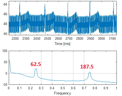
Whenever we try to acquire the ECG channels in this configuration, the signals appears very noisy. The analysis of the signals power spectrum shows different peaks at specific frequencies as shown by the following figure: 

These peaks are always present regardless the environment noise or the channel analysed. 

Is this caused by the ADS or we doing something wrong? Anyone else noticed this behaviour? 

Thanks.

  • Hello Rudy,

    You are seeing power line frequency interference which is extremely common in biomedical applications. Every application will have to deal with this problem at some point or another.

    The ADS1298 is equipped with an internal Right-Leg Drive amplifier which has the capability to sense common-mode signals on the inputs and output a cancellation signal that can be applied to the patient. This can significantly reduce interference from the power line due to the interference's common-mode nature.

    However, using the RLD amplifier is not quite enough to completely eliminate power line interference in some applications. In those, digital filters are implemented in the microcontroller to further attenuate the noisy unwanted signals.

    Regards,
    Brian Pisani
  • Hi Brian and thank you very much for your feedback.

    The system we developed is powered by a LiPo battery and the laptop used to read data from the microcontroller was not connected to the AC supply. All the tests were performed in relatively low-noise environments. Moreover, please also note that the power line frequency in my country is 50Hz.

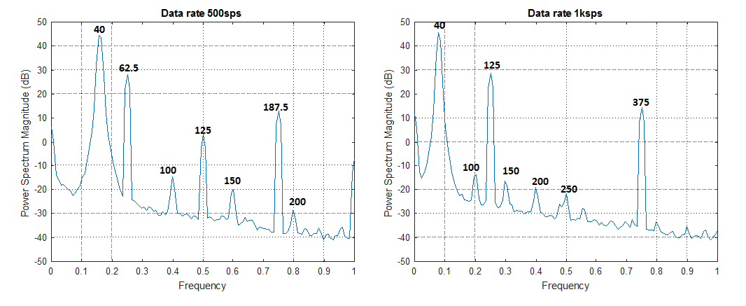
    We also noted that similar peaks are shifted to higher frequencies if the output data rate is increase. Here is the power spectrum at 1000sps (unfiltered vs. 2nd order digital filter). Seems that data rate and those peaks are somehow related.

    untitled.png

    Thanks.

  • Hey Rudy,

    Can you send me your schematic? Could you try inputting a 40 Hz sine wave to one of the channels at the 500 SPS data rate and then again at 1kSPS and analyze the spectrum to see if it appears at 40 Hz each time? This will rule out a bug in the code.

    Brian
  • Hi Brian,

    we made the test you suggested and these are the results we got:

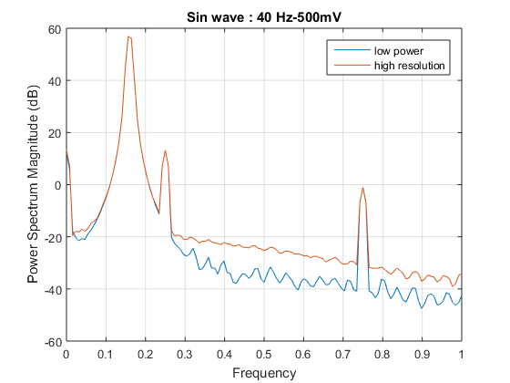
    The power of the 40Hz sine wave is predominant, however we can still notice those peaks at the same frequencies as before: 65.5Hz and 187.5Hz for 500sps and 125Hz and 375Hz for 1000sps. (We used a wave generator connected to AC power, thus it is now possible to see the power supply interference as well)

    I have attached here the schematic and the register configuration we are using. Maybe we made a mistake into that or we are missing something important into the ADS functionality.

    Thank you very much for your support Brian.

    Rudy

    ads1298_lib.c
    /* ========================================
     *
     * Copyright YOUR COMPANY, THE YEAR
     * All Rights Reserved
     * UNPUBLISHED, LICENSED SOFTWARE.
     *
     * CONFIDENTIAL AND PROPRIETARY INFORMATION
     * WHICH IS THE PROPERTY OF your company.
     *
     * ========================================
    */
    
    #include "ads1298_lib.h"
    
    void set_all_ads1298_reg (TADS1298REGS * all_reg)
    {
        /*---------------------------------------*/
        /*config1 register*/
        /*---------------------------------------*/   
        all_reg->config1.control_bit.reserved=0;
        all_reg->config1.control_bit.hr=HIGH_RESOLUTION; //high resolution mode
        all_reg->config1.control_bit.daisyen=0; //daisy chain disabled
        all_reg->config1.control_bit.clken=0; //oscillator clock output disable
            
        all_reg->config1.control_bit.rsv=0;
        
        all_reg->config1.control_bit.dr=HR_500SPS; //500SPS
        /*---------------------------------------*/
        
        /*---------------------------------------*/
        /*config 2*/
        /*---------------------------------------*/
        all_reg->config2.control_bit.rsv7=0;
        all_reg->config2.control_bit.wct_chop=0; //wct chopping freq fixed
        all_reg->config2.control_bit.inttest=1; //test signal are generated internally
        all_reg->config2.control_bit.rsv3=0;
        all_reg->config2.control_bit.testamp=0; // calib signal amplitude 1 mV
        all_reg->config2.control_bit.testfreq=0b00;//0b00; // fclck/2^21     //0b10; //not used         //11 dc   
        /*---------------------------------------*/
        
        /*---------------------------------------*/
        /*config 3*/
        /*---------------------------------------*/    
        all_reg->config3.control_bit.pdbrefbuf=1; //enable internal reference buffer
        all_reg->config3.control_bit.rsv6=1; //reserved must be 1
        all_reg->config3.control_bit.vref4v=0; // internal reference set at 2.4V
        all_reg->config3.control_bit.rldmeas=0; // measuring RLD
        all_reg->config3.control_bit.rldrefint=0; //rld_ref at (Avdd-avss)/2
        all_reg->config3.control_bit.pdbrld=0; //RLD buffer
        all_reg->config3.control_bit.rldloffsens=0; //rld sense
        all_reg->config3.control_bit.rldstat=0; // rld is connected   
        /*---------------------------------------*/ 
        
        /*---------------------------------------*/
        /*LOFF*/
        /*---------------------------------------*/       
        all_reg->loff.control_bit.compth=0b000; //thresghold @ 95%/5%
        all_reg->loff.control_bit.vleadoffen=0; //current source mode lead off
        all_reg->loff.control_bit.ileadoff=0b00; //6nA
        all_reg->loff.control_bit.fleadoff=0b10; //not use at the moment
        /*---------------------------------------*/ 
        
        /*---------------------------------------*/
        /*ch1set*/
        /*---------------------------------------*/
        all_reg->ch1set.control_bit.pd=0; //normal operation
        all_reg->ch1set.control_bit.gain=GAIN_6; // PGA gain = 6
        all_reg->ch1set.control_bit.rsv=0; //reserved must be 0
        all_reg->ch1set.control_bit.mux=INPUT_ELECTRODE; // test signal   //0b000; // normal electrod input
        /*---------------------------------------*/
        
        /*---------------------------------------*/
        /*ch2set*/
        /*---------------------------------------*/
        all_reg->ch2set.control_bit.pd=0; //normal operation
        all_reg->ch2set.control_bit.gain=GAIN_6; // PGA gain = 6
        all_reg->ch2set.control_bit.rsv=0; //reserved must be 0
        all_reg->ch2set.control_bit.mux=INPUT_ELECTRODE; // normal electrod imput
        /*---------------------------------------*/
        
        /*---------------------------------------*/
        /*ch3set*/
        /*---------------------------------------*/
        all_reg->ch3set.control_bit.pd=0; //normal operation
        all_reg->ch3set.control_bit.gain=GAIN_6; // PGA gain = 6
        all_reg->ch3set.control_bit.rsv=0; //reserved must be 0
        all_reg->ch3set.control_bit.mux=INPUT_ELECTRODE; // normal electrod imput
        /*---------------------------------------*/
        
        /*---------------------------------------*/
        /*ch4set*/
        /*---------------------------------------*/
        all_reg->ch4set.control_bit.pd=0; //normal operation
        all_reg->ch4set.control_bit.gain=GAIN_6; // PGA gain = 6
        all_reg->ch4set.control_bit.rsv=0; //reserved must be 0
        all_reg->ch4set.control_bit.mux=INPUT_ELECTRODE; // normal electrod imput
        /*---------------------------------------*/
        
        /*---------------------------------------*/
        /*ch5set*/
        /*---------------------------------------*/
        all_reg->ch5set.control_bit.pd=0; //normal operation
        all_reg->ch5set.control_bit.gain=GAIN_6; // PGA gain = 6
        all_reg->ch5set.control_bit.rsv=0; //reserved must be 0
        all_reg->ch5set.control_bit.mux=INPUT_ELECTRODE; // normal electrod imput
        /*---------------------------------------*/
        
        /*---------------------------------------*/
        /*ch6set*/
        /*---------------------------------------*/
        all_reg->ch6set.control_bit.pd=0; //normal operation
        all_reg->ch6set.control_bit.gain=GAIN_6; // PGA gain = 6
        all_reg->ch6set.control_bit.rsv=0; //reserved must be 0
        all_reg->ch6set.control_bit.mux=INPUT_ELECTRODE; // normal electrod imput
        /*---------------------------------------*/
        
        /*---------------------------------------*/
        /*ch7set*/
        /*---------------------------------------*/
        all_reg->ch7set.control_bit.pd=0; //normal operation
        all_reg->ch7set.control_bit.gain=GAIN_6; // PGA gain = 6
        all_reg->ch7set.control_bit.rsv=0; //reserved must be 0
        all_reg->ch7set.control_bit.mux=INPUT_ELECTRODE; // normal electrod imput
        /*---------------------------------------*/
        
        /*---------------------------------------*/
        /*ch8set*/
        /*---------------------------------------*/
        all_reg->ch8set.control_bit.pd=0; //normal operation
        all_reg->ch8set.control_bit.gain=GAIN_6; // PGA gain = 6
        all_reg->ch8set.control_bit.rsv=0; //reserved must be 0
        all_reg->ch8set.control_bit.mux=INPUT_ELECTRODE; // normal electrod imput
        /*---------------------------------------*/    
        
        /*---------------------------------------*/
        /*rld_sensp*/
        /*---------------------------------------*/    
        all_reg->rldsensp.value=0;
        /*---------------------------------------*/ 
        
        /*---------------------------------------*/
        /*rld_sensn*/
        /*---------------------------------------*/    
        all_reg->rldsensn.value=0;
        /*---------------------------------------*/
        
        /*---------------------------------------*/
        /*loff_sensp*/
        /*---------------------------------------*/
        all_reg->loffsensp.value=0xFF;
        /*---------------------------------------*/
        
        /*---------------------------------------*/
        /*loff_sensn*/
        /*---------------------------------------*/
        all_reg->loffsensn.value=0x02;
        /*---------------------------------------*/    
        
        /*---------------------------------------*/
        /*loff_flip*/
        /*---------------------------------------*/
        all_reg->loffflip.value=0x00;
        /*---------------------------------------*/
        
        /*---------------------------------------*/
        /*GPIO*/
        /*---------------------------------------*/
        all_reg->gpio.value=0x0F; //input
        /*---------------------------------------*/
        
        /*---------------------------------------*/
        /*PACE*/
        /*---------------------------------------*/
        all_reg->pace.control_bit.rsv=0b000;
        all_reg->pace.control_bit.pacee=0b00; //2 channel
        all_reg->pace.control_bit.paceo=0b00; //channel 1
        all_reg->pace.control_bit.pdpace=0; //buffer turned off
        /*---------------------------------------*/
        /*---------------------------------------*/
        /*RESP*/
        /*---------------------------------------*/
        all_reg->resp.value=0; //no respiration
        /*---------------------------------------*/
    
        /*---------------------------------------*/
        /*CONFIG4*/
        /*---------------------------------------*/
        all_reg->config4.control_bit.freq=0b000;
        all_reg->config4.control_bit.rsv4=0; //must be 0
        all_reg->config4.control_bit.singleshot=0; //continous conversion mode
        all_reg->config4.control_bit.wcttorld=0; //connection off
        all_reg->config4.control_bit.pdbloffcomp=0; // lead off comparator disabled    
        /*---------------------------------------*/    
        
        /*---------------------------------------*/
        /*WCT1*/
        /*---------------------------------------*/    
        all_reg->wct1.control_bit.avfch6=0;
        all_reg->wct1.control_bit.avlch5=0;
        all_reg->wct1.control_bit.avrch7=0;
        all_reg->wct1.control_bit.avrch4=0;
        all_reg->wct1.control_bit.pdwcta=1; //wcta powered on
        all_reg->wct1.control_bit.wcta=0b010; // channel 2 positive in connected to wcta
        /*---------------------------------------*/
        
        /*---------------------------------------*/
        /*WCT2*/
        /*---------------------------------------*/
        all_reg->wct2.control_bit.pdwctc=1; //wctc powered on
        all_reg->wct2.control_bit.pdwctb=1; //wctb powered on
        all_reg->wct2.control_bit.wctb=0b100; // channel 3 positive
        all_reg->wct2.control_bit.wctc=0b011; // channel 2 negative    
        /*---------------------------------------*/
        
        return;
    }


    /* [] END OF FILE */
    
    ads1298_lib.h

    SMS_Med v1.2 REV2 schematic.pdf

  • Hi Rudy,

    Brian is tied up most of today, so I thought I would make a few suggestions in the meantime.

    The 2 dominant tones you saw initially occurred at fDATA/8 and 3*fDATA/8, both for fDATA = 500SPS and fDATA = 1kSPS (500SPS: OSR = 1024, 1kSPS: OSR = 512). It looks like the frequency of the tones is not affected by the OSR. Have you tried changing the master clock (CLK) or modulator clock (fMOD) frequency instead? There are a couple ways you might try this:

    1. If you are using the internal oscillator, you could repeat these tests in Low-Power Mode by setting CONFIG1[7] = 0. LP Mode decreases fMOD by 1/2. You could test the same data rates in LP Mode using OSR = 256 for 1kSPS and OSR = 512 for 500SPS.
    2. If you have access to an external clock source, you could also try sweeping the CLK frequency for a given configuration and see if this affects the tones. The allowable CLK input range is from 1.94MHz to 2.25MHz.

    When you run these tests, I would first configure the channels for internal input short (MUXn[2:0] = 001) and power-down any unused channels. Then, configure the channels normally and apply several different DC inputs (say 100mV, 500mV, 1V, etc) with Gain set to 1 to see if the tones are coupling through the inputs somehow.

    Best Regards,

  • Hi Ryan,

    thanks for your help. Great to get so much support for your side, we are really struggling to make our system work properly.

    We make the test you suggested and these are the results:

    This is the result of the HR mode vs. LP mode test (500sps). LR seems better (in general it looks like there's less noise), but when it comes to the unwanted peaks, they are still there. It seems that fMOD is not affecting the acquisition or causing the problem.

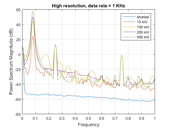
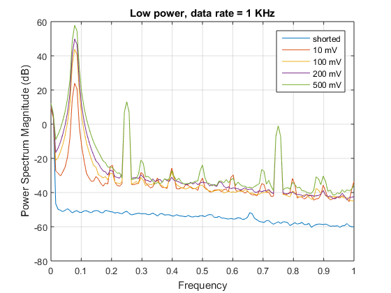
    We also tried to set internal input short for channel 2 and to power-down all the other unused channels. The result is shown by the blue line of the following plots. In this case there are no peaks.

    After that, we tried to acquire a 40Hz sine wave at different amplitudes (10mV, 100mV, 100mV and 500mV). In this case nothing changed, and the peaks are always part of the calculated power spectrum. 

    The test was repeated in LP mode and with a data rate of 500sps. 

    In all the test we made, the gain was set to 1 as suggested.

  • Hi Rudy,

    After reviewing your results, I would agree that the issue does not seem related fMOD or the data rate. You may still want to try using a different CLK frequency from an external clock source if you can - that's the only other detail which has remained constant so far. The idea is to see if the tones shift at all in amplitude or in frequency.

    The only clear relationship that I see is that the tones disappear for VIN = 0V and reappear for anything greater than 0V. Since you've tried multiple input sources (the ECG source and the function generator), I wonder if the tones are coupling through the reference voltage. From the schematic, it looks like you are using the internal reference. How close is that 10uF cap (C30) to the reference pins? Are you able to squeeze another cap in parallel (i.e. 0.1uF)? Ideally, the smaller cap would be placed as close to the device as possible, directly across the VREFP and VREFN pins, to help decouple any noise from the reference node.

    A couple other questions that may lead us somewhere:

    1. Does the LiPo battery supply AVDD and DVDD directly, or is there another power conditioning stage before the ADS1298?
    2. Are there any other clocks or switching devices on your board? Can any of them be powered down while you acquire data?

    Best Regards,

  • Hi Rudy - could you send us your complete register settings? I'd like to review those and see if there's anything else we might have overlooked.

    Thanks,
  • Hi Ryan,

    sorry my late reply. The complete register setting we are using is attached here. Regarding the other suggestions, these are my comments:

    1. As you suggested, we will try to use an external clock source to see if something changes. 

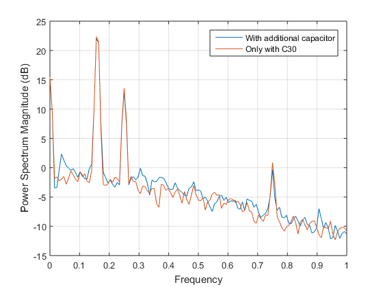
    2. The capacitor C30 is actually quite close to the ADS1298 (just few mm). Anyway, we tried to add a parallel capacitor (0.1uF) close to ADS. The result is shown by the following power spectrum. Unfortunately it didn't make a big difference.

    3. The battery that supplies all the components of the circuit is actually placed in a separate module. Inside this module there's a voltage regulator to regulate the battery voltage to 3.3V. We do not have a real difference between AVDD and DVDD, both of them are set to 3.3V.

    4. The Cypress microcontroller we are using to acquire data from the ADS1298 is placed on the same PCB (ADS is on the top layer, µC on the bottom layer). We did try to shut down the microcontroller and to acquire the ECG data through another microcontroller placed on a separate board, however it didn't make any difference. We also tried to change the SPI clock and the internal clock frequency of the microcontroller, no effect on the peaks.

    Thank you.

    Best,

    3487.ads1298_lib.c
    /* ========================================
     *
     * Copyright YOUR COMPANY, THE YEAR
     * All Rights Reserved
     * UNPUBLISHED, LICENSED SOFTWARE.
     *
     * CONFIDENTIAL AND PROPRIETARY INFORMATION
     * WHICH IS THE PROPERTY OF your company.
     *
     * ========================================
    */
    
    #define HIGH_RESOLUTION     1
    #define HR_500SPS           0b110    
    #define GAIN_6              0b000    
    #define INPUT_ELECTRODE     0b000
    
    
    void set_all_ads1298_reg (TADS1298REGS * all_reg)
    {
        /*---------------------------------------*/
        /*config1 register*/
        /*---------------------------------------*/   
        all_reg->config1.control_bit.reserved=0;
        all_reg->config1.control_bit.hr=HIGH_RESOLUTION; 
        all_reg->config1.control_bit.daisyen=0; 
        all_reg->config1.control_bit.clken=0;        
        all_reg->config1.control_bit.rsv=0;    
        all_reg->config1.control_bit.dr=HR_500SPS; //500 SPS
        /*---------------------------------------*/
        
        /*---------------------------------------*/
        /*config 2*/
        /*---------------------------------------*/
        all_reg->config2.control_bit.rsv7=0;
        all_reg->config2.control_bit.wct_chop=0; 
        all_reg->config2.control_bit.inttest=1; 
        all_reg->config2.control_bit.rsv3=0;
        all_reg->config2.control_bit.testamp=0; 
        all_reg->config2.control_bit.testfreq=0b00;  
        /*---------------------------------------*/
        
        /*---------------------------------------*/
        /*config 3*/
        /*---------------------------------------*/    
        all_reg->config3.control_bit.pdbrefbuf=1; 
        all_reg->config3.control_bit.rsv6=1;
        all_reg->config3.control_bit.vref4v=0; 
        all_reg->config3.control_bit.rldmeas=0; 
        all_reg->config3.control_bit.rldrefint=0; 
        all_reg->config3.control_bit.pdbrld=0; 
        all_reg->config3.control_bit.rldloffsens=0; 
        all_reg->config3.control_bit.rldstat=0;
        /*---------------------------------------*/ 
        
        /*---------------------------------------*/
        /*LOFF*/
        /*---------------------------------------*/       
        all_reg->loff.control_bit.compth=0b000; 
        all_reg->loff.control_bit.vleadoffen=0; 
        all_reg->loff.control_bit.ileadoff=0b00; 
        all_reg->loff.control_bit.fleadoff=0b10; //not use at the moment
        /*---------------------------------------*/ 
        
        /*---------------------------------------*/
        /*ch1set*/
        /*---------------------------------------*/
        all_reg->ch1set.control_bit.pd=0; 
        all_reg->ch1set.control_bit.gain=GAIN_6; 
        all_reg->ch1set.control_bit.rsv=0; 
        all_reg->ch1set.control_bit.mux=INPUT_ELECTRODE; 
        /*---------------------------------------*/
        
        /*---------------------------------------*/
        /*ch2set*/
        /*---------------------------------------*/
        all_reg->ch2set.control_bit.pd=0; 
        all_reg->ch2set.control_bit.gain=GAIN_6; 
        all_reg->ch2set.control_bit.rsv=0; 
        all_reg->ch2set.control_bit.mux=INPUT_ELECTRODE; 
        /*---------------------------------------*/
        
        /*---------------------------------------*/
        /*ch3set*/
        /*---------------------------------------*/
        all_reg->ch3set.control_bit.pd=0; 
        all_reg->ch3set.control_bit.gain=GAIN_6; 
        all_reg->ch3set.control_bit.rsv=0; 
        all_reg->ch3set.control_bit.mux=INPUT_ELECTRODE; 
        /*---------------------------------------*/
        
        /*---------------------------------------*/
        /*ch4set*/
        /*---------------------------------------*/
        all_reg->ch4set.control_bit.pd=0; 
        all_reg->ch4set.control_bit.gain=GAIN_6; 
        all_reg->ch4set.control_bit.rsv=0; 
        all_reg->ch4set.control_bit.mux=INPUT_ELECTRODE; 
        /*---------------------------------------*/
        
        /*---------------------------------------*/
        /*ch5set*/
        /*---------------------------------------*/
        all_reg->ch5set.control_bit.pd=0; 
        all_reg->ch5set.control_bit.gain=GAIN_6; 
        all_reg->ch5set.control_bit.rsv=0; 
        all_reg->ch5set.control_bit.mux=INPUT_ELECTRODE; 
        /*---------------------------------------*/
        
        /*---------------------------------------*/
        /*ch6set*/
        /*---------------------------------------*/
        all_reg->ch6set.control_bit.pd=0; 
        all_reg->ch6set.control_bit.gain=GAIN_6; 
        all_reg->ch6set.control_bit.rsv=0; 
        all_reg->ch6set.control_bit.mux=INPUT_ELECTRODE; 
        /*---------------------------------------*/
        
        /*---------------------------------------*/
        /*ch7set*/
        /*---------------------------------------*/
        all_reg->ch7set.control_bit.pd=0;
        all_reg->ch7set.control_bit.gain=GAIN_6; 
        all_reg->ch7set.control_bit.rsv=0; 
        all_reg->ch7set.control_bit.mux=INPUT_ELECTRODE; 
        /*---------------------------------------*/
        
        /*---------------------------------------*/
        /*ch8set*/
        /*---------------------------------------*/
        all_reg->ch8set.control_bit.pd=0; 
        all_reg->ch8set.control_bit.gain=GAIN_6; 
        all_reg->ch8set.control_bit.rsv=0; 
        all_reg->ch8set.control_bit.mux=INPUT_ELECTRODE; 
        /*---------------------------------------*/    
        
        /*---------------------------------------*/
        /*rld_sensp*/
        /*---------------------------------------*/    
        all_reg->rldsensp.value=0;
        /*---------------------------------------*/ 
        
        /*---------------------------------------*/
        /*rld_sensn*/
        /*---------------------------------------*/    
        all_reg->rldsensn.value=0;
        /*---------------------------------------*/
        
        /*---------------------------------------*/
        /*loff_sensp*/
        /*---------------------------------------*/
        all_reg->loffsensp.value=0xFF;
        /*---------------------------------------*/
        
        /*---------------------------------------*/
        /*loff_sensn*/
        /*---------------------------------------*/
        all_reg->loffsensn.value=0x02;
        /*---------------------------------------*/    
        
        /*---------------------------------------*/
        /*loff_flip*/
        /*---------------------------------------*/
        all_reg->loffflip.value=0x00;
        /*---------------------------------------*/
        
        /*---------------------------------------*/
        /*GPIO*/
        /*---------------------------------------*/
        all_reg->gpio.value=0x0F; 
        /*---------------------------------------*/
        
        /*---------------------------------------*/
        /*PACE*/
        /*---------------------------------------*/
        all_reg->pace.control_bit.rsv=0b000;
        all_reg->pace.control_bit.pacee=0b00; 
        all_reg->pace.control_bit.paceo=0b00; 
        all_reg->pace.control_bit.pdpace=0; 
        /*---------------------------------------*/
        /*---------------------------------------*/
        /*RESP*/
        /*---------------------------------------*/
        all_reg->resp.value=0; //no respiration
        /*---------------------------------------*/
    
        /*---------------------------------------*/
        /*CONFIG4*/
        /*---------------------------------------*/
        all_reg->config4.control_bit.freq=0b000;
        all_reg->config4.control_bit.rsv4=0; 
        all_reg->config4.control_bit.singleshot=0; 
        all_reg->config4.control_bit.wcttorld=0; 
        all_reg->config4.control_bit.pdbloffcomp=0; 
        /*---------------------------------------*/    
        
        /*---------------------------------------*/
        /*WCT1*/
        /*---------------------------------------*/    
        all_reg->wct1.control_bit.avfch6=0;
        all_reg->wct1.control_bit.avlch5=0;
        all_reg->wct1.control_bit.avrch7=0;
        all_reg->wct1.control_bit.avrch4=0;
        all_reg->wct1.control_bit.pdwcta=1; 
        all_reg->wct1.control_bit.wcta=0b010; 
        /*---------------------------------------*/
        
        /*---------------------------------------*/
        /*WCT2*/
        /*---------------------------------------*/
        all_reg->wct2.control_bit.pdwctc=1; 
        all_reg->wct2.control_bit.pdwctb=1; 
        all_reg->wct2.control_bit.wctb=0b100; 
        all_reg->wct2.control_bit.wctc=0b011;     
        /*---------------------------------------*/
        
        return;
    }
    
    
    /* [] END OF FILE */
    

  • Hi Rudy,

    Thank you for providing the updates. I realize we've been trying several different tests to isolate the problem, so thank you for your patience as well.

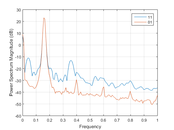
    I reviewed your register settings and found that you are using a reserved setting in the LOFF register. The valid settings for FLEAD_OFF[1:0] are only "01" (fDR/4) and "11" (DC). Currently, you are using "10," which we do not support. Try changing this setting to one of the two supported options and see if this cleans up the noise. If you do not plan to use lead-off detection at all, you can disable the lead-off detection for each individual input in the LOFF_SENSP/N registers.

    Best Regards,

  • Hi Ryan,

    I am finally able to report back with the results we got from your last suggestion. I am happy to say that the change into the register setting solve the problem as you can see from the plots here below.


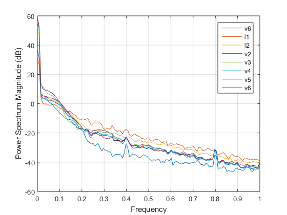
    Here below also the power spectrum of a real ECG acquisition:

    Once again, thank you very much for the support, Ryan!! In case of any other future issue while developing, I will open a new thread.

    All the best,

    Rudy