This thread has been locked.

If you have a related question, please click the "Ask a related question" button in the top right corner. The newly created question will be automatically linked to this question.

ADS1158: Data apparently incorrect in some cases while measuring a fixed DC signal

Part Number: ADS1158
Other Parts Discussed in Thread: REF5025, REF5040, ADS1258, ADS1262

in our analog circuit, I found there was some cases that incorrect data were derived from ADS1158.

Thus, I use Tektronix function generator to generate a  300 mv signal. And I use channel AIN5 (0xD) of ADS1158 to measure it.

VREF: 4.96V

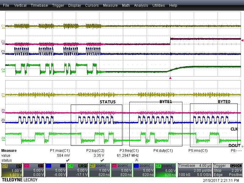
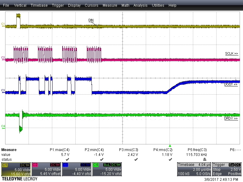
I useed a gpio pin to trigger the scope while the abnormal case happened.

in normal case, adc count are 2238~2278. (298.4mv ~  303.73mv)

but in abnormal case, i got the big count, and it was not spi interface problem or calculation problem.

Because in scope, the signal output from ADS1158 actually sent that big value on DOUT pin

please check

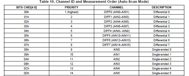
STATUS BYTE: 0x8D  (NEW & CHID = AIN5)

DATA BYTE1: 0x51

DATA BYTE0: 0x8C

data = 0x518C = 20876 --> 2783mv    !!

and C1 is measured signal, from scope, its max is P1: max(C1) = 584mv

Please give some clues about this scenario. thanks

regards,

             Ivan


  • Hi Ivan,

    Thanks for providing the scope shots!

    I'm curious what commands you're sending on DIN during data retrieval? The reason I ask is that 0x8C would be a reasonable value for a status byte.


    Other information that would would be helpful to me for troubleshooting this issue would be:

    • What data rate are you running the ADS1158 at?

    • Are you reading data with the Channel Data Read Command (0x30) or the Channel Data Read Direct (0x00)?

    • Are you using fixed channel-mode or auto-scan mode?

      • If using auto-scan mode, do you have other channels enabled?


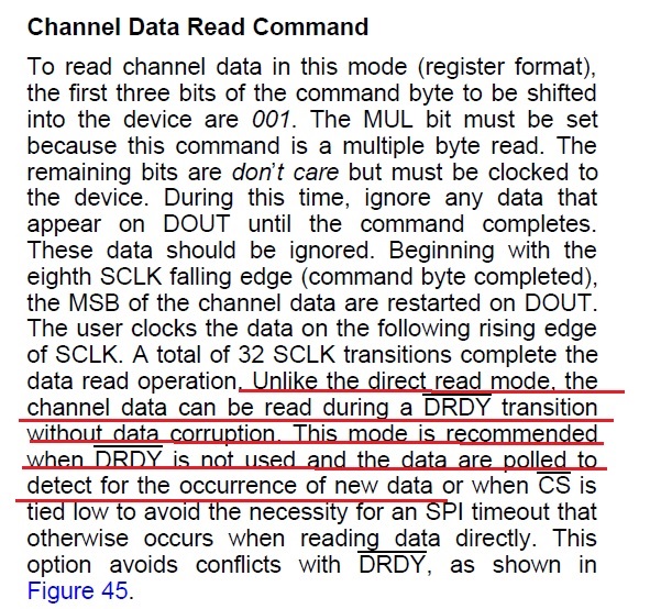
    I would suggest reading with the Channel Data Read Command (0x30), since it does not require you to toggle chip select and you can read data during a /DRDY transition. Reading data during a /DRDY transition with the Channel Data Read Direct (0x00) command can result in corrupted data.


    Best Regards,
    Chris 

  •  The reason I ask is that 0x8C would be a reasonable value for a status byte

    --> why?  in my test, CHID[0:4] = 0xD is correct, meaning AIN5, isnt it?

    add required info

    0. I use polling method to get ADS1158 data. AND START pin is always pulled to HIGH after ADC initialization to make data conversion.

    If I find NEW bit of status byte is set, the following two data are new and valid. Otherwise, ignore and discard the data.

    1. Usechannel read command to get the data, i.e.,  Channel Data Read Command (0x30), and enable MULT_REG_ACCESS

    for data rate, i only set DLY[2:0] to 010 in the initialization.  DRATE[1:0] = 11 (default value)

    2. use auto-scan mode (default)

    3. I have other channel enabled. total 6 singled ended input are enabled, respectively, S0, S1, S2,S3,S4, S5. I only take S5 result for the experiment.

    I would suggest reading with the Channel Data Read Command (0x30), since it does not require you to toggle chip select and you can read data during a /DRDY transition

    ==>

    4. I attached parts of codes. please check if something wrong.  I assert CS low in the beginning of reading data, and deasserted CS in the end of reading

    5. Another strange thing is that, I found OVF bit of status bit is sometimes set (rarely). I dont know the reason. I am sure that input is not overflowed (4.096V)

    I just discard the data.

    if any further information is required and helpful, please let  me know.

    void spi_xmit(Uint16 a);
    
    
    // ADS1158 Initial Configuration
    void ADS1158Config(void) {
    //	unsigned int temp = 0;
    
    	ADS1158Reset();
    
    	ADS1158SetSwitchDelay(ADS1158_DELAY_2);
    
    	ADS1158SetChannel(  ADS1158_MUX_S0    |
    						ADS1158_MUX_S1    |
    						ADS1158_MUX_S2    |
    						ADS1158_MUX_S3    |
    						ADS1158_MUX_S4    |
    						ADS1158_MUX_S5    );
    
    }
    
    
    void ADS1158AssertCS(int fAssert) {
    
        if (fAssert) {
            GpioDataRegs.GPBCLEAR.bit.GPIO57 = 1;
            DELAY_US(1);
        } else{
        	DELAY_US(5);
        	GpioDataRegs.GPBSET.bit.GPIO57 = 1;
        }
    }
    
    void ADS1158SendByte(unsigned char Byte) {
        unsigned char dummy = 0;
    
        spi_xmit(Byte);
    
        while (SpiaRegs.SPISTS.bit.INT_FLAG != 1) {
        } // Wait until RX data is ready
        dummy = SpiaRegs.SPIRXBUF;
    
    }
    
    unsigned char SPIReceiveByte(void) {
        unsigned char Result = 0;
    
        Result = SpiaRegs.SPIRXBUF; // Read RXBUF to clear INT_FLAG
    
        spi_xmit(0xFFFF); //send out NOP to generate SCLK
    
        while (SpiaRegs.SPISTS.bit.INT_FLAG != 1) {
        } // Wait until RX data is ready
        Result = SpiaRegs.SPIRXBUF;
    
    
        return Result;
    }
    /*
     ******************************************************************************
     higher level functions
     */
    void ADS1158ReadData(Uint16* status, long* Data) {
        //long Data;
    	unsigned int adcCode[3] = {0};
        // assert CS to start transfer
    
    	//disable MCU interrupt
    	DINT;
    
        ADS1158AssertCS(1);
    
        // send the command byte
        ADS1158SendByte(ADS1158_CMD_CH_RDATA | ADS1158_CMD_MULT_REG_ACCESS);
    
        // get the conversion result
    
        *status = SPIReceiveByte();
        adcCode[0] = SPIReceiveByte();
        adcCode[1] = SPIReceiveByte();
        if (adcCode[0] & 0x80) {
              *Data = (long)(0xff) << 24;
          }
          *Data = *Data | ((long)(adcCode[0] & 0xff) << 8 );
          *Data = *Data | ((long)(adcCode[1] & 0xff) << 0 );


        // de-assert CS
        ADS1158AssertCS(0);
        //return Data;
    	
    	//enable back interrupt
        EINT;
        ERTM;
    
    	//debugging: trigger scope
        if (*Data > 5000 && (*status == 0x8D) ) {
              GpioDataRegs.GPASET.bit.GPIO13 = 1;
              DELAY_US(10000);
              GpioDataRegs.GPACLEAR.bit.GPIO13 = 1;
              asm("        ESTOP0");
        }
    
    
    }
    
    void ADS1158ReadRegister(int StartAddress, int NumRegs, unsigned * pData) {
        int i;
        // assert CS to start transfer
        ADS1158AssertCS(1);
    
        if ( NumRegs > 1) {
    		// send the command byte
    		ADS1158SendByte(ADS1158_CMD_RREG | ADS1158_CMD_MULT_REG_ACCESS | (StartAddress & 0xf));
        } else {
        	// send the command byte
    		ADS1158SendByte(ADS1158_CMD_RREG | (StartAddress & 0xf));
        }
    
        // get the register content
        for (i = 0; i < NumRegs; i++) {
            *pData++ = SPIReceiveByte();
        }
    
        // de-assert CS
        ADS1158AssertCS(0);
    
        return;
    }
    
    void ADS1158WriteRegister(int StartAddress, int NumRegs, unsigned * pData) {
        int i;
    
        // assert CS to start transfer
        ADS1158AssertCS(1);
    
        // send the command byte
        if ( NumRegs > 1) {
    		// send the command byte
    		ADS1158SendByte(ADS1158_CMD_WREG | ADS1158_CMD_MULT_REG_ACCESS | (StartAddress & 0xf));
        } else {
        	// send the command byte
    		ADS1158SendByte(ADS1158_CMD_WREG | (StartAddress & 0xf));
        }
    
        // send the data bytes
        for (i = 0; i < NumRegs; i++) {
            ADS1158SendByte(*pData++);
        }
    
        // de-assert CS
        ADS1158AssertCS(0);
    
        return;
    }
    
    void ADS1158Reset(void) {
    
    	// Reset Converter
    	GpioDataRegs.GPBCLEAR.bit.GPIO51 = 1;
    
    
        DELAY_US(10);	//delay at lease 2 Tclk <=  1 us
        GpioDataRegs.GPBSET.bit.GPIO51 = 1; // Active Low --> Set High initially
    
        return;
    }
    
    int ADS1158SetChannel(Uint32  Mux) {
    
    	unsigned int mux_diff = ( Mux & 0x000000ff );
    	unsigned int mux_sg1  = ( Mux & 0x0000ff00 ) >> 8;
    	unsigned int mux_sg2  = ( Mux & 0x00ff0000 ) >> 16;
    	unsigned int mux_sys  = ( Mux & 0xff000000 ) >> 24;
    
    	ADS1158WriteRegister(ADS1158_3_REGISTER_MUXDIF, 1, &mux_diff);
    	ADS1158WriteRegister(ADS1158_4_REGISTER_MUXSG0, 1, &mux_sg1);
    	ADS1158WriteRegister(ADS1158_5_REGISTER_MUXSG1, 1, &mux_sg2);
    	ADS1158WriteRegister(ADS1158_6_REGISTER_SYSRED, 1, &mux_sys);
    
    
        return ADS1158_NO_ERROR;
    }
    
    int ADS1158SetDataRate(int DataRate) {
        unsigned Temp;
    	ADS1158ReadRegister(ADS1158_1_REGISTER_CONFIG1, 0x01, &Temp);
    	Temp &= 0xfc;	// strip out old settings
    	Temp = Temp + DataRate;
        // write the register value containing the new value back to the ADS
        ADS1158WriteRegister(ADS1158_1_REGISTER_CONFIG1, 0x01, &Temp);
    	ADS1158ReadRegister(ADS1158_1_REGISTER_CONFIG1, 0x01, &Temp);


        return ADS1158_NO_ERROR;
    }
    
    int ADS1158SetSwitchDelay(int delay) {
        unsigned Temp;
    	ADS1158ReadRegister(ADS1158_1_REGISTER_CONFIG1, 0x01, &Temp);
    	Temp &=  0x8f;	// strip out old settings
    	Temp = Temp + delay;
        // write the register value containing the new value back to the ADS
        ADS1158WriteRegister(ADS1158_1_REGISTER_CONFIG1, 0x01, &Temp);
    	ADS1158ReadRegister(ADS1158_1_REGISTER_CONFIG1, 0x01, &Temp);


        return ADS1158_NO_ERROR;
    }
    

  • Hi Chris,

                      in hardware consideration of ADS1158 spec, power supply needs

    If our circuit does not use a LDO to supply the ADS1158, is it possible to have the issue I described earlier?

    that is, AVDD have a ripple (> 2mv)

    We didnt pay much attention to this because in most time ADC seems to work well.

    regards,

               Ivan

  • Chris,

               welcome for any comment..

    regards,

                 Ivan

  • Hi Ivan,

    Sorry for the delayed response...

    Regarding the supply noise, not filtering the switching supply with an LDO could result in a more noisy ADC conversion result; however, I doubt it would cause the issue you're seeing.

    I looked through your code and I did find a couple of potential problems:

    1) I would recommend clearing out the "Data" variable before assigning a new value to it. Also, bits 16-23 need to be included in the sign-extension of the 32-bit data type, as shown below:

    *Data = 0; // Ensure that there is no residual value still stored in "Data".
    if (adcCode[0] & 0x80) {
        *Data = (long)(0xff) << 24;
        *Data = *Data | ((long)(0xff) << 16 ); // Don't forget to sign-extend this byte as well
    }
    *Data = *Data | ((long)(adcCode[0] & 0xff) << 8 );
    *Data = *Data | ((long)(adcCode[1] & 0xff) << 0 );

    2) In your "SPIReceiveByte()" function it looks like you might be sending two bytes and only retrieving one of them:

    unsigned char SPIReceiveByte(void) {
        unsigned char Result = 0;
        Result = SpiaRegs.SPIRXBUF; // Read RXBUF to clear INT_FLAG
        spi_xmit(0xFFFF); //send out NOP to generate SCLK // Is this clocking out 2 bytes?
        // NOTE: As a best practice, I would recommend sending "0x00" when clocking out data.
        while (SpiaRegs.SPISTS.bit.INT_FLAG != 1) {
        } // Wait until RX data is ready
        Result = SpiaRegs.SPIRXBUF; return Result;
    }


    Additionally, I might suggest the following things to try to debug the issue:

    1. Try decreasing the ADC's data rate to see if this helps resolve the communication issue. Decreasing the data rate increases the time between conversions and often relaxes the SPI timing requirements. Sometimes you'll see SPI communications issues go away at lower data rates. If so, this can be a good clue that points to an SPI timing violation.

    2. Your previous oscilloscope screenshot did show some noise on the SPI signals. While SPI is fairly immune to noise, I might still recommend placing some 50-100 series resistors on the SPI signals to help reduce digital edge rates and provide some noise filtering (in conjunction with the parasitic capacitances on each trace).

    3. You might try configuring the ADS1158 in fixed-channel mode for this test and see if you still see the issue. That way you'll know that the ADC is not automatically multiplexing between input channels.


    Regarding the OVF bit in the STATUS byte, are any of your other selected input channels floating or possibly over-ranged? Also, what are you using to provide the reference voltage to the ADS1158?

    You might also want to inspect the reference voltage to ensure that it is stable. If your reference voltage is drooping, it could also cause this type of error (and the conversion result error).


    Best Regards,
    Chris

  • Hi Chris,   

                  Thanks for your opinion. I will try what you suggest.

    But I think it is not issue about the communication or SPI problem, right? What I saw in the scope (ADC's DOUT) is the same as what I caught in the program (MCU). 

    Later I will update the result I try with the fixed channel and a more stable power supply for ADC.

    2) In your "SPIReceiveByte()" function it looks like you might be sending two bytes and only retrieving one of them:

    --> it exactly send one byte (I will change it to send 0x00 to generate clk)  

    what are you using to provide the reference voltage to the ADS1158?

      --> use a LDO with 4.096V

  • Hi Ivan,

    To be honest I'm a bit confused by the oscilloscope results. It would be be nice to see the /DRDY and DIN signals as well to get a better idea of what may be happening. You might also try decreasing the data rate to see if the outliers go away. Many times when there is an SPI timing issue you may notice issues occurring at the faster data rates.

    It might also be a good idea to probe the reference voltage to make sure it is stable and free of glitches. It's odd to see an LDO used for the reference, typically you would want a more precise voltage reference source (something like the REF5025).

    Best Regards,
    Chris
  • It might also be a good idea to probe the reference voltage to make sure it is stable and free of glitches. It's odd to see an LDO used for the reference, typically you would want a more precise voltage reference source (something like the REF5025).

    Actually, I use TI REF5040 for ref voltage.

    To be honest I'm a bit confused by the oscilloscope results. It would be be nice to see the /DRDY and DIN signals as well to get a better idea of what may be happening. You might also try decreasing the data rate to see if the outliers go away. Many times when there is an SPI timing issue you may notice issues occurring at the faster data rates.

    => because I use polling method and NEW bit of status byte, I didnt monitor the state of DRDY.

    If it is possible, I'll send you another scope snapshot with more information (DRDY/DIN)

  • Hi Ivan,

    The REF5040 should work well since it is a buffered referenced, and polling /DRDY should also be okay as long as you use the read data command.

    Do you have a schematic of your circuit that you could share?
    I'm starting to wonder if there might be something external to the ADC which could be causing the odd behavior. For example, inductors on the supply pins can cause voltage spike during current transients or a large impedance between the analog and digital grounds of the ADC can result in the analog and digital grounds being at different voltage potentials.

    Thanks,
    Chris
  • Hi Chris,

               Do you have a schematic of your circuit that you could share?

               ==> Please refer to this post. Just replace ADS1258 with ADS1158. use AIN0 as input

    <e2e.ti.com/.../1970975

    regards,

                     Ivan

  • Hi Ivan,

    I would try two things:

    • Try removing the L1 and L2 inductors and replacing them with 0-Ohm resistors. A series inductor and shunt capacitor can form an LC resonator. Also, any fast transient currents can cause large voltage spikes across the inductors. For these reasons, I generally do not recommend using inductors in passive filters.

    • Try adding differential filter capacitors between your ADC inputs. The ADC inputs are switched-capacitor and an external capacitor can provide a more stable input voltage when the inputs are switching.

    Best Regards,
    Chris

  • Try adding differential filter capacitors between your ADC inputs. The ADC inputs are switched-capacitor and an external capacitor can provide a more stable input voltage when the inputs are switching.

    I am not very clear about this action. Could you explain in more details? AIN0 used singled-ended measurement in our test

    regards,

                   Ivan

  • Hi Chris,

    Try adding differential filter capacitors between your ADC inputs. The ADC inputs are switched-capacitor and an external capacitor can provide a more stable input voltage when the inputs are switching.

                     Could you draw a brief diagram about that? thanks

    regards,

                    Ivan

  • Hi Ivan,

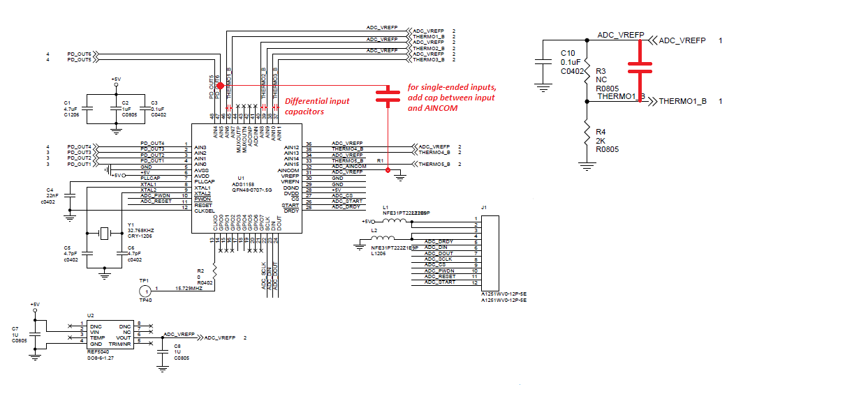
    Here's an example using the circuit you referenced:

    For differential inputs, insert a cap between the positive and negative inputs, in this case it looks like you're measuring between ADC_VREFP and THERMO1_B.

    For single-ended measurements, do the same thing but treat AINCOM as the "negative input". By treating the single-ended signal like it's differential, you can help reduce common-mode impedance coupling between various parts of the circuit.

    These capacitors should be placed close to the ADC for best performance.

    Best Regards,
    Chris

  • Hi Chris,

                    do some works, and try what you recommend to do. However, they does not seem to work for my problem

    - Try decreasing the ADC's data rate to see if this helps resolve the communication issue

    - You might try configuring the ADS1158 in fixed-channel mode for this test and see if you still see the issue

    - Try removing the L1 and L2 inductors and replacing them with 0-Ohm resistors. A series inductor and shunt capacitor can form an LC resonator. Also, any fast transient currents can cause large voltage spikes across the inductors. For these reasons, I generally do not recommend using inductors in passive filters.

    - Try adding differential filter capacitors between your ADC inputs

    any further advices??

    regards,

                   ivan

  • To be honest I'm a bit confused by the oscilloscope results. It would be be nice to see the /DRDY and DIN signals as well to get a better idea of what may be happening

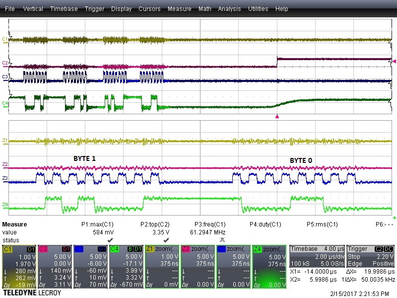
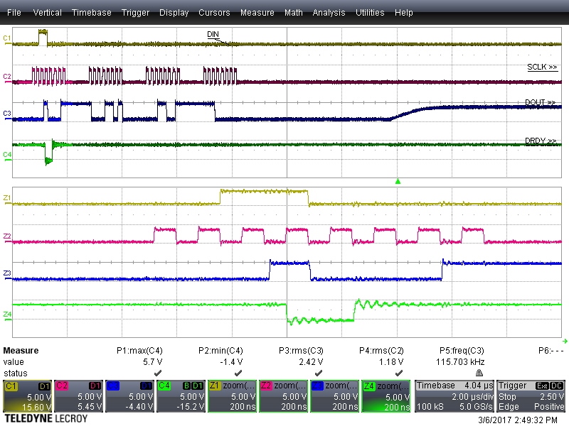
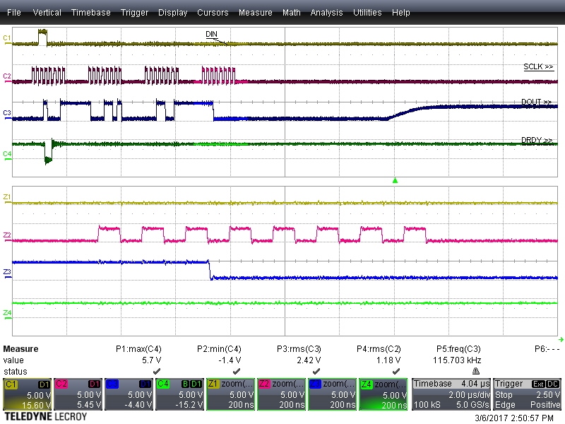
    ==>  for your confuse, I do the same test again. The correct value should be 0.3v (adc cnt should be about 2250). In this case, we occasionally got the cnt = 6624 (0x19E0)

    We use DRATE: 0b11, switch delay: 2, automatic scanning (AIN0 & AIN1 & AIN2 & AIN3 & AIN4 & AIN5)

    what we see on the scope is AIN5, thus status byte is 0x8D (NEW + CHID = 0xD)

    whole 4 bytes:

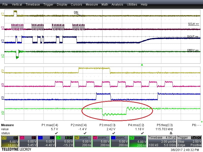
    Zoom View of COMMAND BYTE (Z1: DIN, Z2: SCLK, Z3: DOUT, Z4:DRDY)

    Zoom View of DATA BYTE1:

    Zoom View of Data Byte 2

    we apply the following recommendation from you, still had the same problem

    1. improve AVDD & DVDD of ADS1158 (remove inductors,  and dont use switching power, supplied by IC REG104-5 )

    2. add  cap in input filtering sample current

    3. decrease data rate

    4. use fixed channel

    any comment?

  • Hi Chris,

                   I think I have solved the issue. But I still have some confuse about that.

    From my ealier scope snapshot of COMMAND BYTE (channel data read 0x30), you can see DRDY had a transition from high to low.

    I found in my errorenous case, DRDY had a transition while my channel data read command was sent.

    Thus, I just check DRDY state before I read data from ADS1158.  If DRDY is low, do reading from ADS1158 to avoid DRDY transition during channel reading.

    In result, the issue does not happen anymore. But spec says different things.

    thanks.

    regards,

                    Ivan

  • Hi Ivan,

    Currently, I'm not sure if the SPI command (input) can be sent during a /DRDY transition or if it is just the data bytes (output) that can occur during a /DRDY transition. Our digital designer is currently out of office, but I will discuss this with him when he's back next week.

    Best regards,
    Chris
  • Hi Ivan,

    I discussed this with our digital designer and it turns out that the timing of the RDATA command is important...

    When you send the RDATA command it loads the conversion result into an output shift register. When you clock out this data, it will not get corrupted when new data becomes available. However, if you happen to send the RDATA command while the next conversion is completing (during the /DRDY falling edge), the output shift register will get loaded with data that is a combination of old and new data.

    To avoid this issue, the best solution would be to monitor /DRDY and read the data soon after the conversion completes. However, if you're polling /DRDY then my suggestion would be to make sure that you're polling often enough (2-4 times faster than the data rate) so that you're able to read the data sooner (before the next /DRDY) falling edge.

    Best regards,
    Chris
  • Christopher Hall said:


    To avoid this issue, the best solution would be to monitor /DRDY and read the data soon after the conversion completes.

    Best regards,
    Chris

    hi Chris,

                  It does not seem to make sense. In some cases, MCU cannot immediately handle Interrupt handler (handling other interrupts with higher priority) even if using a interrupt (not polling) for DRDY.

    In most case, MCU can send RDATA command to read back converted data as soon as DRDY falling low. However, it is possible that MCU is busy doing

    other jobs while DRDY is fallling low. While MCU completes other jobs and try to send RDATA to read, the next conversion might be completing....

    Data might be corrupted in this case

    Right?

    regards,

                 Ivan

  • Hi Ivan,

    You are correct, even if you are using interrupts, the MCU may be busy with other tasks or may be interrupted by higher priority tasks. Generally, speaking, as a system designer you will always have to make decisions about which tasks need to be the highest priority and how much of a load your MCU can handle. This can be especially challenging when trying to use an ADC with fast data rates to achieve high data throughput!

    In the case of the ADS1158, the read data command will help protect data from corruption once you've sent the first command byte. Therefore, you will need to ensure that you are able to issue this command soon after the /DRDY interrupt, well in advance of the next /DRDY. There are probably several different ways to enforce this, but one example solution could be to set up two different interrupts:

    1. The first interrupt can occur when the MCU detects a falling edge on /DRDY. This interrupt should be a high priority. When servicing this interrupt, you should quickly issue a read data command and then trigger a second (lower priority) interrupt to finish reading the data. Note that /CS should be held low until you've finished clocking out all of the data.

    2. The second interrupt can be a lower priority; however, you'll want to make sure that it is serviced fast enough such that i) the ADS1158 does not incur an SPI timeout and 2) is too slow that you're not able to read the next conversion result in time (causing a loss of data). When called, this interrupt clocks out the remaining data bytes. This part of the data read can occur during a /DRDY falling edge without any data corruption.

    I hope that helps,
    Chris
  • Hi Chris,

                    Understood what you mention. But, the result seems to be different from what the spec says..

    The spec says channel data read will not corrupt the data with/without DRDY...

    Is there the same issue in other ADC using DRDY or channel read command? for example ADS1258 or ADS1262..etc..

    regards,

                  Ivan

  • Hi Ivan,

    I agree that the datasheet is not very clear on this. Using the read data command is more robust than than the read data direct mode; however, the command must still be decoded by the device before the next /DRDY falling edge.

    Our newer devices, like the ADS1262, do not have this issue. I believe there is a double buffered output that prevents data corruption. However, if you're in the situation where your reading data near the /DRDY falling edge, it can be hard to determine which result you are reading (the previous one or the newest one). Therefore, it's always best practice to make sure you have sufficient time to read the data before the next conversion result.

    Some other possible solutions to prevent data corrupt or data loss would be to:

    - Decrease the data rate. Reading data so close to the end of the conversion is putting you at risk of losing the conversion result altogether. Therefore, if you don't the higher throughput you might as well take advantage of the loser noise performance of a slower data rate.

    - Yet another option would be to use pulse convert mode. If you are only monitoring a signal which doesn't require a consistent sampling rate, you could use pulse convert mode to collect data only when your processor is ready for it.

    Best regards,
    Chris