This thread has been locked.

If you have a related question, please click the "Ask a related question" button in the top right corner. The newly created question will be automatically linked to this question.

ADS8363: ADS8363 reads garbage output data

Part Number: ADS8363

Hello all,

I am trying to read data from ads8363 converter. I am able to write/read configuration register, but when it comes to reading adc readings I am getting all kinds of seemingly of random values, sometime correct values, sometimes some random data.

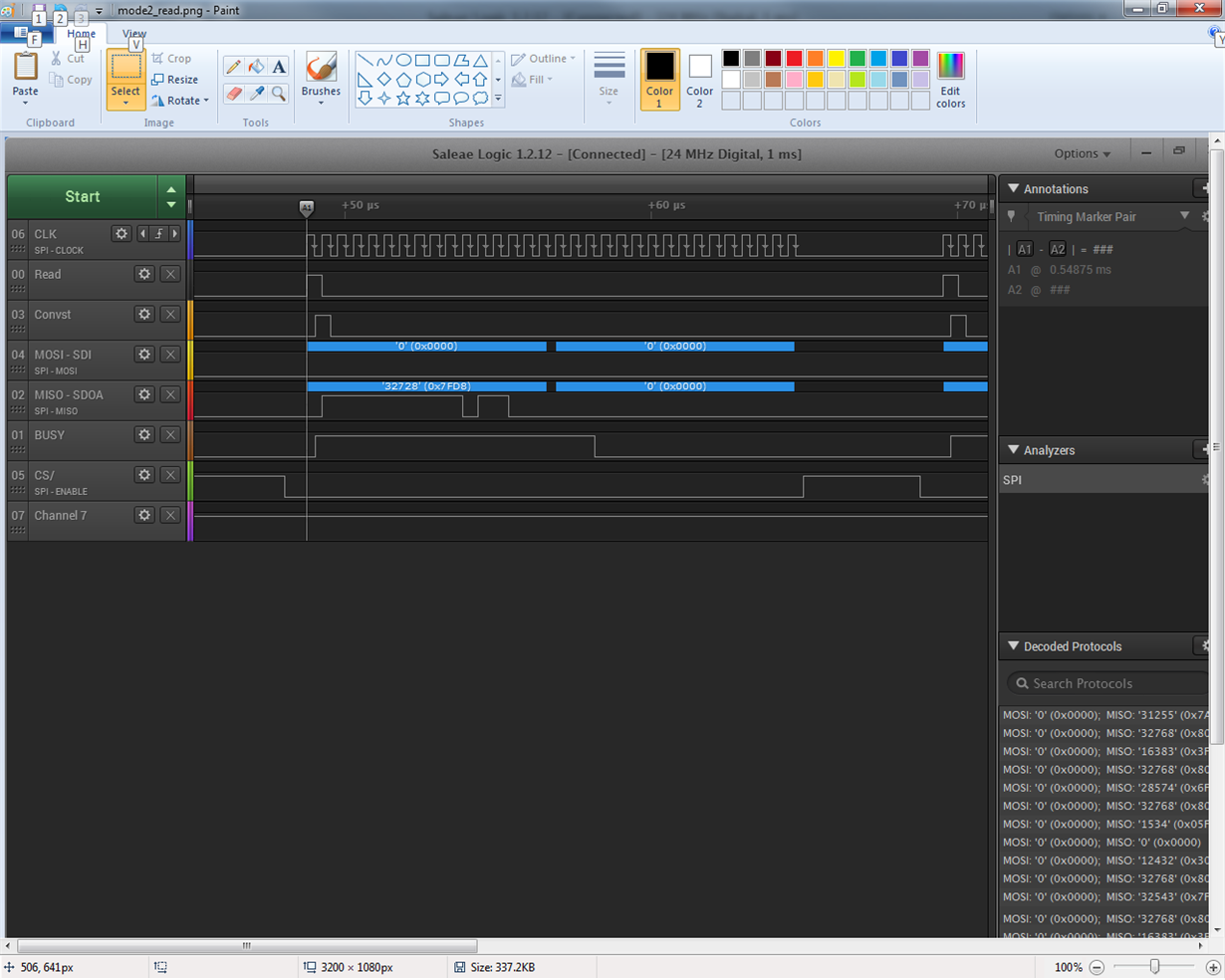
I am attaching here the file from the logic analyzer, I have doubts about my CONVST and RD signals. I set them up such that RD always come half-clock earlier than CONVST.

In my setup the RD signal is triggered by the raising edge of the first clock-pulse, and the RD lasts for one clock cycle. The CONVST starts on the falling edge of the first clock, half clock cycle later, and also lasts for one clock-cycle.

Is this OK ?

( I work in MODE II - M0=0, M1=1, with only SDOA active).

Regards, George.

  • The conversion cycle starts from the assertion of CONVST. During the conversion, the results of the previous conversion can be read. When RD is asserted, the ADC clocks out the first MSB. The problem with your setup happens because in your waveforms, RD is asserted before CONVST. When a new conversion begins, the data in the output registers gets updated with the new result. Reading data during the start of the conversion causes you to be reading some of the old result and some of the new result, which looks like garbage output data.

    Moving RD to be just after CONVST will fix your problems.
  • Bryan, thanks ! This solved the problem for me. I put the RD and CONVST in the opposite order - CONVST starts first, and RD comes half clock cycle later. Now I read constant data.
  • Bryan, it turns out that my happiness was premature.

    When I set the RD and CONVST signals so that the have identical timing - I still get the garbage data. If you look in the timing diagram in my original message, I shifted the CONVST half clock behind so that now it starts exactly with RD. With this set-up I still get garbage data.
    But ADS8363 application note states that it has to work when RD and CONVST have identical timing.
  • Bryan, finally I got meaningful readings out of ADS8363. It works with RD and CONVST that have identical timing.

    The problem was in very unexpected place, perhaps you have an explanation for this.

    I worked with registers REFDAC1 and REFDAC2 being set to 0x03FF. According to the manual this turns on internal reference voltage path.
    But with this setting I got the garbage data coming out of ADC.

    I switched the settings of these registers to 0x07FF just to try, and with this setting everything works fine.
    But this supposed to turn OFF the internal reference voltage. By the way the setting of the REFCM that I have is 0xFFF0 where last 4 bits are set to the internal reference mode.

    So there seems to be some problem with the RPD bit of the REFDAC registers.

    Also I noticed something else. When I power the ADS8363 it should wake-up in the default mode. Which is for the REFDAC1 and REFDAC2 is 0x07FF and this should have internal reference disabled, and pins REFIO1 and REFIO2 should not show the internal reference voltage. But in fact they show this internal reference voltage.

    I tested two different chips and they produce identical results.

    Regards, George.